Method for manufacturing liquid crystal panel, liquid crystal panel and manufacturing system of the same

a technology of liquid crystal panels and manufacturing systems, applied in the direction of identification means, instruments, optics, etc., can solve the problems of large fluctuation in productivity, difficult to deal with diversified products, and inability to deal with product diversification, so as to achieve efficient manufacturing

Inactive Publication Date: 2005-03-22
SHARP KK
View PDF6 Cites 26 Cited by
  • Summary
  • Abstract
  • Description
  • Claims
  • Application Information

AI Technical Summary

Benefits of technology

On the other hand, according to the present invention, although the steps performed in the state of the master glass substrate are common among the liquid crystal panels, steps intrinsic to each liquid crystal panel can be performed in the step o

Problems solved by technology

The inventors of this application consider that the following three problems are inherent in the conventional manufacturing method of the liquid crystal panel.
The first problem is great fluctuation in productivity caused by a dimension of the liquid crystal panel. FIG. 4 shows a relationship between a panel size of the manufacturing line of phase 3 (size of the master glass substrate is 550×650 mm) and th

Method used


Image

  • Method for manufacturing liquid crystal panel, liquid crystal panel and manufacturing system of the same
  • Method for manufacturing liquid crystal panel, liquid crystal panel and manufacturing system of the same
  • Method for manufacturing liquid crystal panel, liquid crystal panel and manufacturing system of the same

Examples


first embodiment

(First Embodiment)

FIG. 5 is a plan view showing in outline a method for manufacturing a liquid crystal panel according to a first embodiment of the present invention; FIG. 6 is a schematic view showing a manufacturing system of a liquid crystal panel; and FIGS. 7A and 7B are plan views respectively showing a master glass substrate and a sub-TFT substrate.

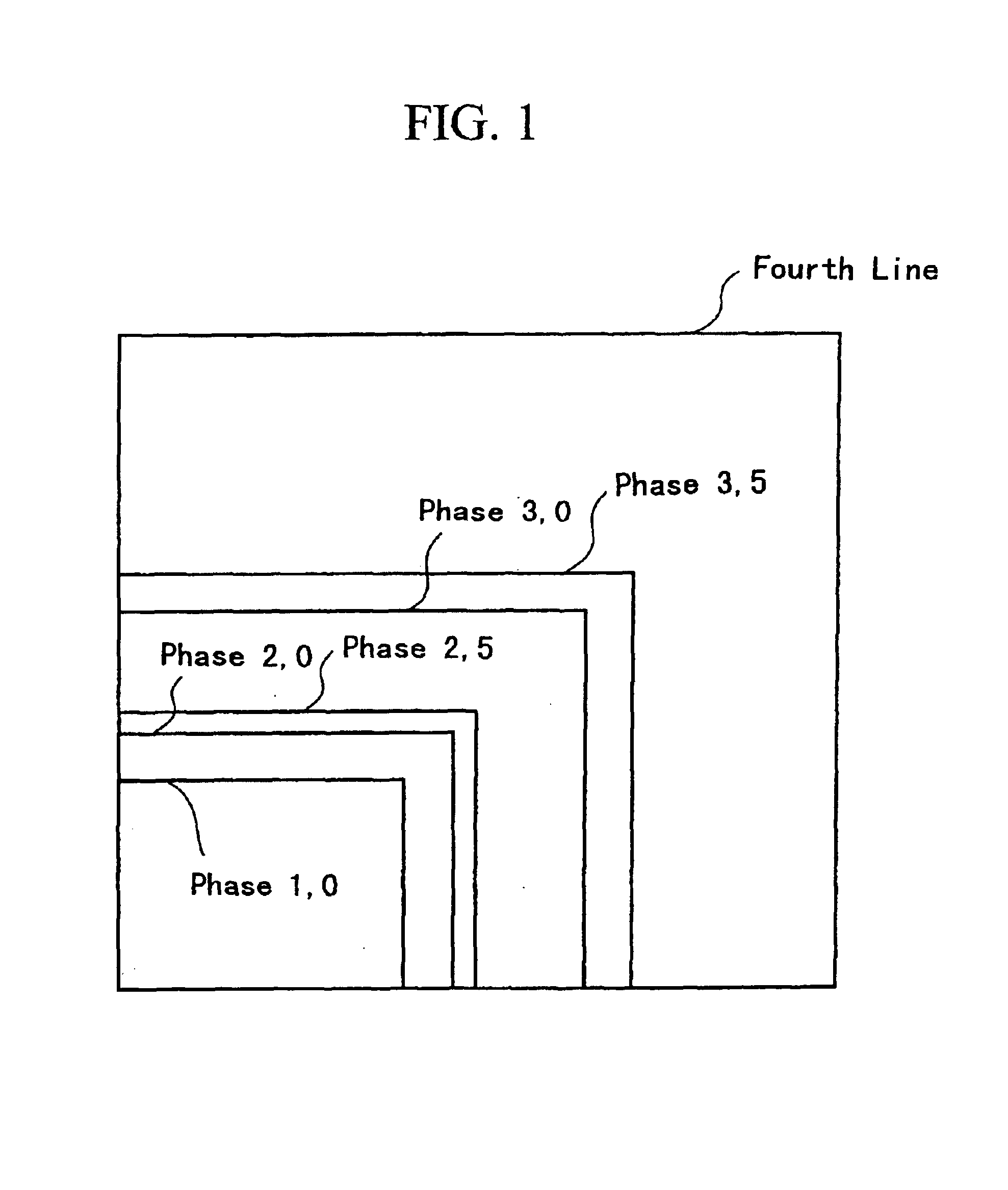
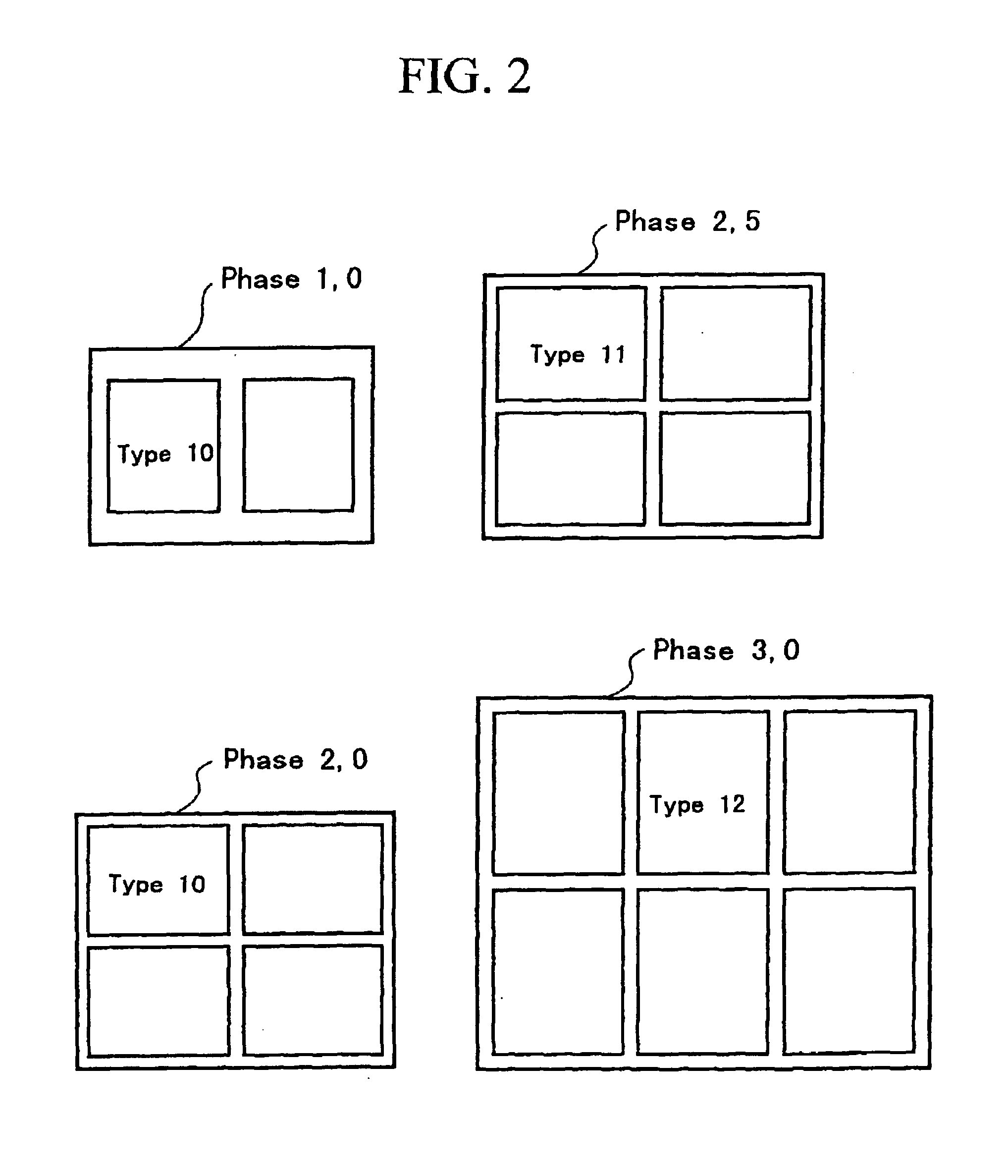
In the first embodiment, a master glass substrate having a size of 960×1000 mm is used. And as shown in FIG. 5, the master glass substrate 10 is plotted into four blocks 11a to 11d. Then, for example, the following regions are secured in the respective blocks: in the first block 11a, one device-forming region 12a for forming a liquid crystal panel of type 20; in the second block 11b, two device-forming regions 12b for forming liquid crystal panels of types 12 to 15; in the third block 11c, four device-forming regions 12c for forming liquid crystal panels of types 10 and 11; and in the fourth block 11d, numerous (six in the drawing) ...

second embodiment

(Second Embodiment)

FIGS. 15A and 15B are views, each of which shows a method for manufacturing a liquid crystal panel according to a second embodiment of the present invention.

In the second embodiment, a master glass substrate 60 is plotted into four blocks 61a to 61d. In an example shown in FIG. 15A, the following regions are secured in each of the blocks 61a to 61d: for example, one device-forming region 62 for forming a liquid crystal panel of type 15 for a monitor; and a plurality of device-forming regions 63 for forming liquid crystal panels of types 2 to 3 for portable telephone sets.

In an example shown in FIG. 15B, for example, the following regions are secured in each of the blocks 61a to 61d: one device-forming region 64 for forming a liquid crystal panel of type 15 for a monitor; and two device-forming regions 65 for forming liquid crystal panels of types 6 to 8 for mobile equipments.

In other words, block division is made for each size of a liquid crystal panel to be manuf...

third embodiment

(Third Embodiment)

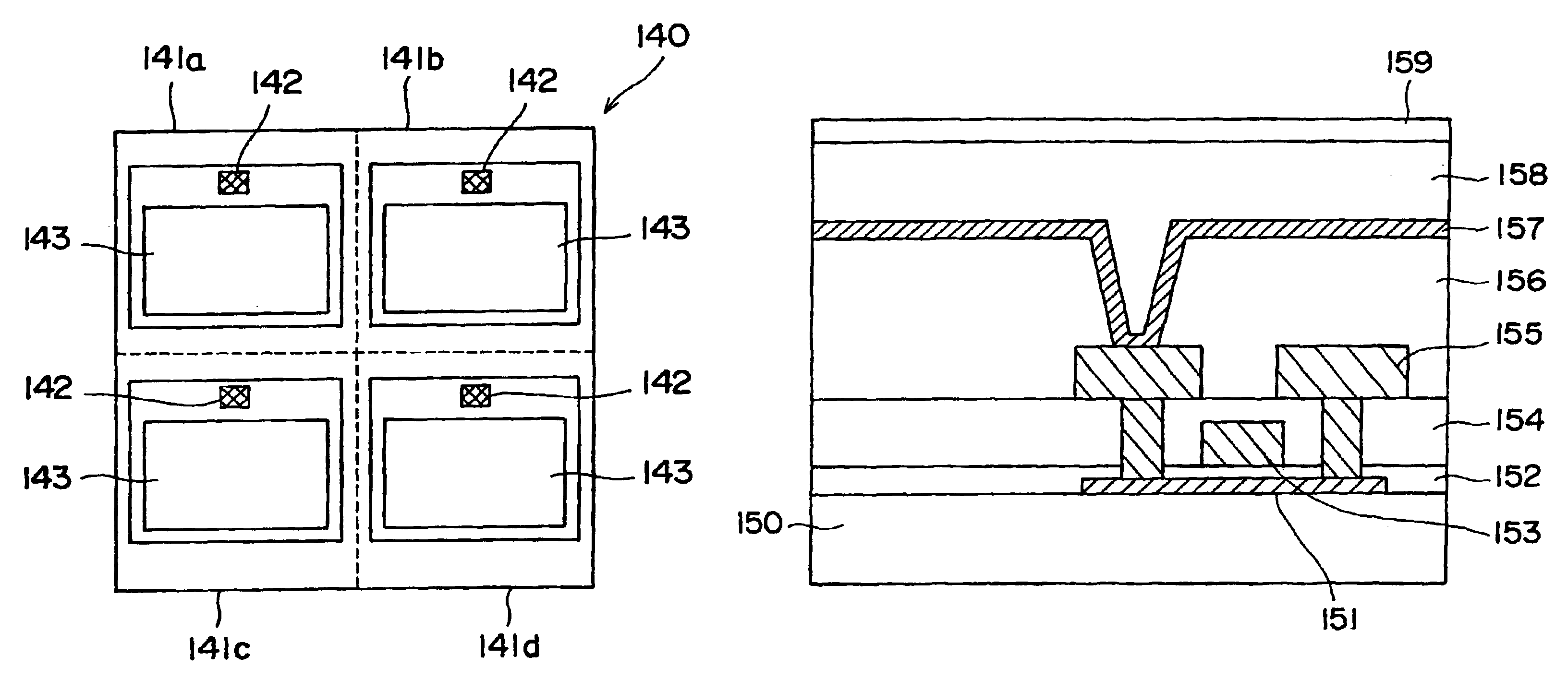
FIG. 16 is a plan view showing in outline a method for manufacturing a liquid crystal panel according to a third embodiment of the present invention. In the third embodiment, a master glass substrate 70 is plotted into four blocks 71a to 71d. The following regions are secured in the respective blocks: in the block 71a, one device-forming region 72a for forming a liquid crystal panel of type 20; in the block 71b, two device-forming regions 72b for forming liquid crystal panels of types 12 to 15; in the block 71c, four device-forming regions 72c for forming liquid crystal panels of types 10 and 11; and in the block 71d, numerous device-forming regions 72d for forming projection panels of a reflection type of type 1.8. A structure of a liquid crystal display panel formed in each of the blocks 71a to 71d is the same as that shown in FIG. 9.

FIG. 17 is a plan view showing a projection panel of a reflection type formed in the block 71d; and FIG. 18 is a sectional view of ...


PUM


Abstract

A substrate is plotted into a plurality of blocks, and each block is plotted into one or a plurality of device-forming regions. By using a first manufacturing line, a conductive film, an insulating film and a semiconductor film which constitute TFT are formed in the device-forming region. Then, primary cutting is performed to cut the substrate into the respective blocks and form a plurality of sub-TFT substrates. Then, by using a second manufacturing line, processing is performed for each sub-TFT substrate in accordance with specifications of a liquid crystal panel to be manufactured. Then, secondary cutting is performed to cut the sub-TFT substrate into respective device-forming regions.

Description

BACKGROUND OF THE INVENTION1. Field of the InventionThe present invention relates to a liquid crystal panel manufacturing method for manufacturing a plurality of liquid crystal panels by using one master glass substrate, a liquid crystal panel manufactured by the manufacturing method and a manufacturing system of the same.2. Description of the Related ArtA display using a liquid crystal panel of an active matrix system prevents crosstalk by providing a switch for each pixel (picture element), the switch being turned OFF at the time of unselection to cut off a signal. Compared with a display using a liquid crystal panel of a simple matrix system, this display shows a better display characteristic. Especially, a liquid crystal display using TFT (Thin Film Transistor) as a switch shows a display characteristic as excellent as that of CRT (Cathode-Ray Tube), because of high driving performance of TFT.Generally, the liquid crystal panel has a structure where a liquid crystal is enclosed ...

Claims


Application Information

Patent Timeline
IPC IPC(8): G02F1/13G02F1/1368G02F1/1333G02F1/136G09F9/00
CPCG02F1/1368G02F1/133351G02F1/136227
Inventor ZHANG, HONGYUNG
Owner SHARP KK
Why Eureka
Try Eureka