Techniques for reducing effects of coupling between storage elements of adjacent rows of memory cells

Inactive Publication Date: 2005-03-22
SANDISK TECH LLC
View PDF26 Cites 223 Cited by
  • Summary
  • Abstract
  • Description
  • Claims
  • Application Information

AI Technical Summary

Benefits of technology

Additional aspects, features and advantages of the present invention can be had from the following detailed description of exemplary embodiments thereof, which description should be read along with reference to the accompanying drawings.

Problems solved by technology

The problem occurs most pronouncedly between two groups of adjacent cells that have been programmed at different times. One group of cells is programmed to add a level of charge to their storage elements that corresponds to one set of data.

Method used


Image

  • Techniques for reducing effects of coupling between storage elements of adjacent rows of memory cells
  • Techniques for reducing effects of coupling between storage elements of adjacent rows of memory cells
  • Techniques for reducing effects of coupling between storage elements of adjacent rows of memory cells

Examples


Embodiment Construction

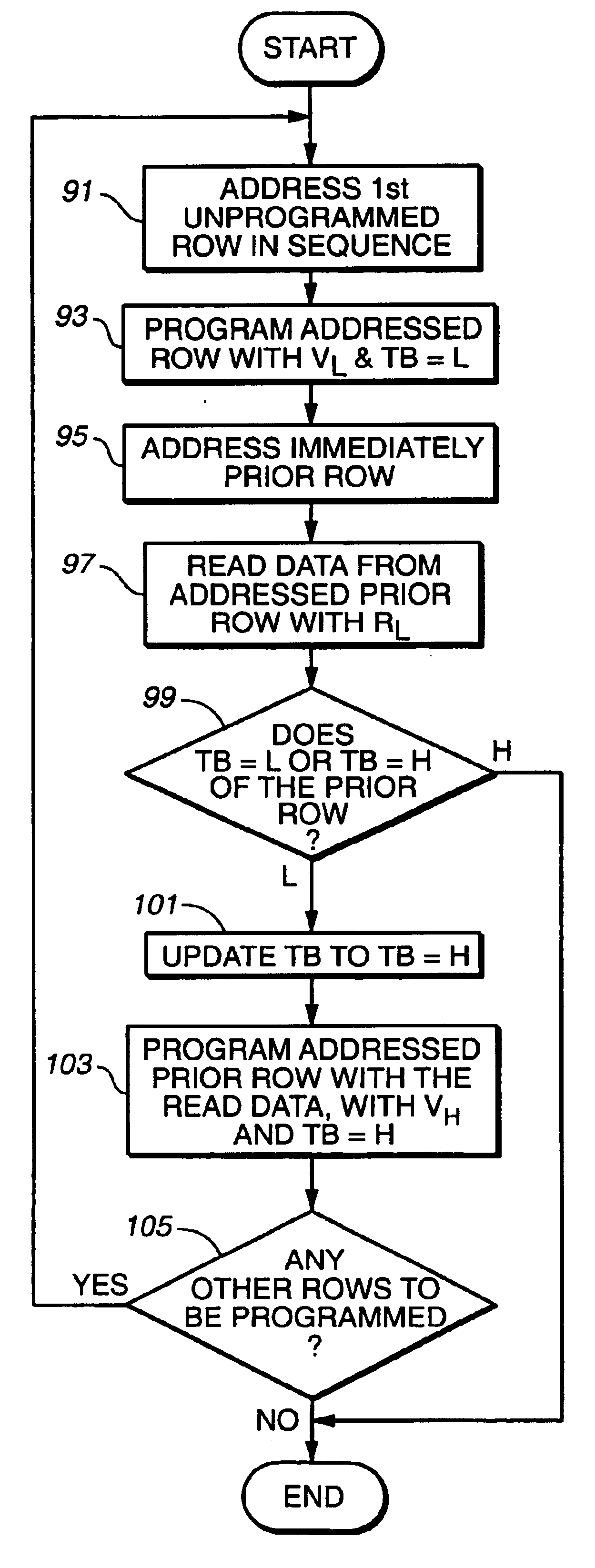
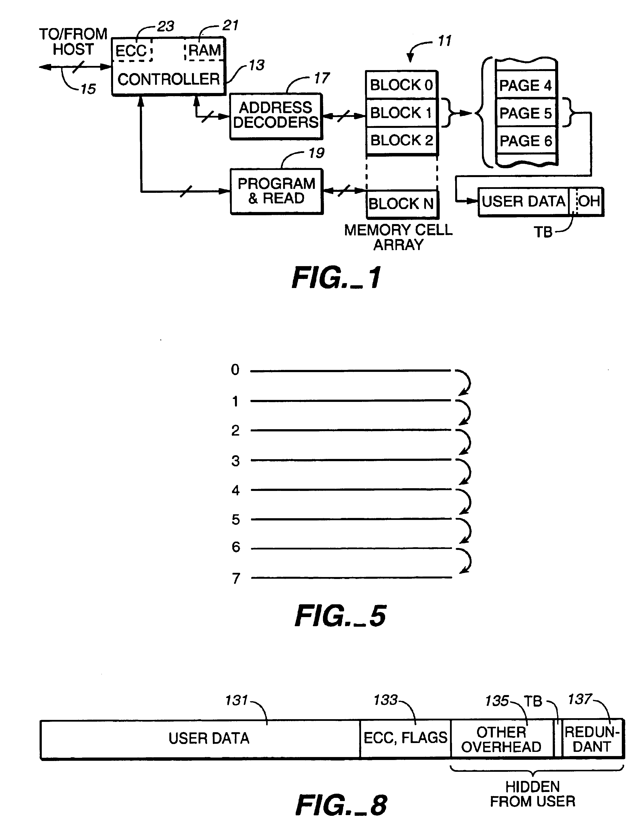
In order to explain the present invention and example implementations, a general diagram of the interrelationship of major components of an example mass memory system is shown in FIG. 1. A primary component of this system is a memory 11, such as an array of memory cells formed on a semiconductor substrate, wherein one or more bits of data are stored in the individual memory cells by storing one of two or more levels of charge on individual storage elements of the memory cells. A non-volatile flash EEPROM is a common type of memory for such systems, and is used in this example.

A second primary component of the memory system of FIG. 1 is a controller 13. The controller 13 communicates over a bus 15 to a host computer or other system that is using the memory system to store data. The controller 13 also controls operation of the memory cell array 11 to write data provided by the host, read data requested by the host and perform various housekeeping functions in operating the memory. The...


PUM


Abstract

Techniques of reducing erroneous readings of the apparent charge levels stored in a number of rows of memory cells on account of capacitive coupling between the cells. All pages of a first row are programmed with a first pass, followed by programming all pages of a second adjacent row with a first pass, after which the first row is programmed with a second pass, and then all pages of a third row are programmed with a first pass, followed by returning to program the second row with a second pass, and so on, in a back-and-forth manner across the rows of an array. This minimizes the effect on the apparent charge stored on rows of memory cells that can occur by later writing data into adjacent rows of memory cells.

Description

FIELD OF THE INVENTIONThis invention relates generally to the field of data memories, and, more specifically, to memories of the type that store data as levels of electronic charge, including, but not limited to, flash electrically erasable and programmable read-only-memories (flash EEPROMs) utilizing either conductive floating gates or dielectric material as charge storage elements.BACKGROUND OF THE INVENTIONIt is common in current commercial products for each storage element of a flash EEPROM array to store a single bit of data by operating in a binary mode, where two ranges of threshold levels of the storage element transistors are defined as storage levels. The threshold levels of transistors correspond to ranges of charge levels stored on their storage elements. In addition to shrinking the size of the memory arrays, the trend is to further increase the density of data storage of such memory arrays by storing more than one bit of data in each storage element transistor. This is...

Claims


Application Information

Patent Timeline
Patent Type & Authority Patents(United States)
IPC IPC(8): G11C11/56G11C16/10G11C16/34G11C16/06G11C16/02
CPCG11C11/5628G11C16/3427G11C16/3418G11C16/10G11C16/12G11C11/56G11C16/34
Inventor CERNEA, RAUL-ADRIANQUADER, KHANDKER N.LI, YANCHEN, JIANFONG, YUPIN
Owner SANDISK TECH LLC
Why Eureka
Try Eureka