Incremental placement of design objects in integrated circuit design

Inactive Publication Date: 2005-03-22
XILINX INC
View PDF5 Cites 26 Cited by
  • Summary
  • Abstract
  • Description
  • Claims
  • Application Information

AI Technical Summary

Benefits of technology

In another embodiment, a plurality of connections of a second type is also received. The connections of the second type are referred to as connections to consider. The connections to consider preferably consist of near-critical connections whose placement d

Problems solved by technology

Additionally, the performance of the circuit may be improved because excess capacitance and resistance caused by long interconnect paths between design objects will slow down the circuit and, in certain cases, delay critical signals and possibly cause functional failures.
As circuits get more complex and device geometry becomes sub-micron, it is rapidly becoming extremely difficult for a human chip designer to manage the complexity of the placement and routing operations.
For example, modern designs contain tens of thousand

Method used


Image

  • Incremental placement of design objects in integrated circuit design
  • Incremental placement of design objects in integrated circuit design
  • Incremental placement of design objects in integrated circuit design

Examples


Embodiment Construction

The present invention relates to a new method of incremental placement. In the following description, numerous specific details are set forth in order to provide a more thorough understanding of the present invention. However, it will be apparent to one skilled in the art that the present invention may be practiced without these specific details. In other instances, well-known features have not been described in detail in order to avoid obscuring the present invention.

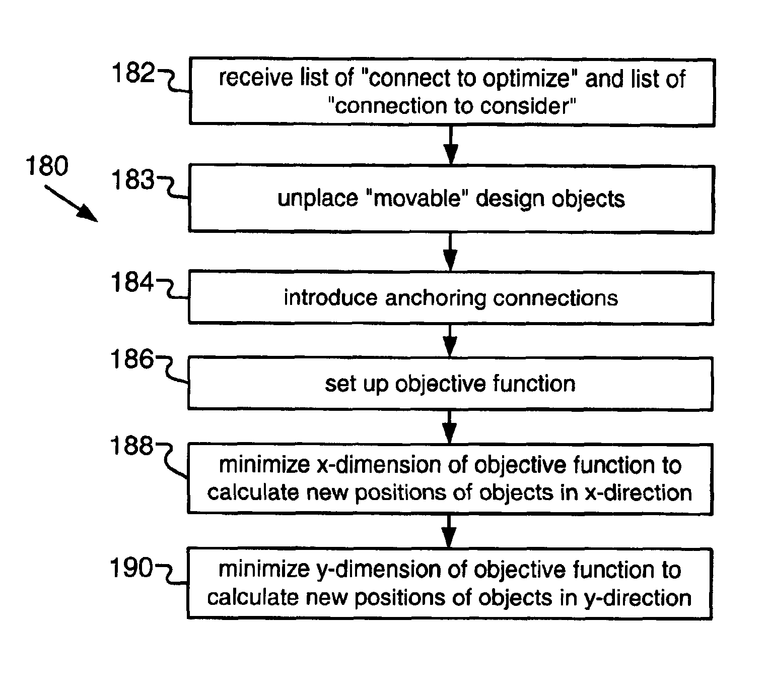
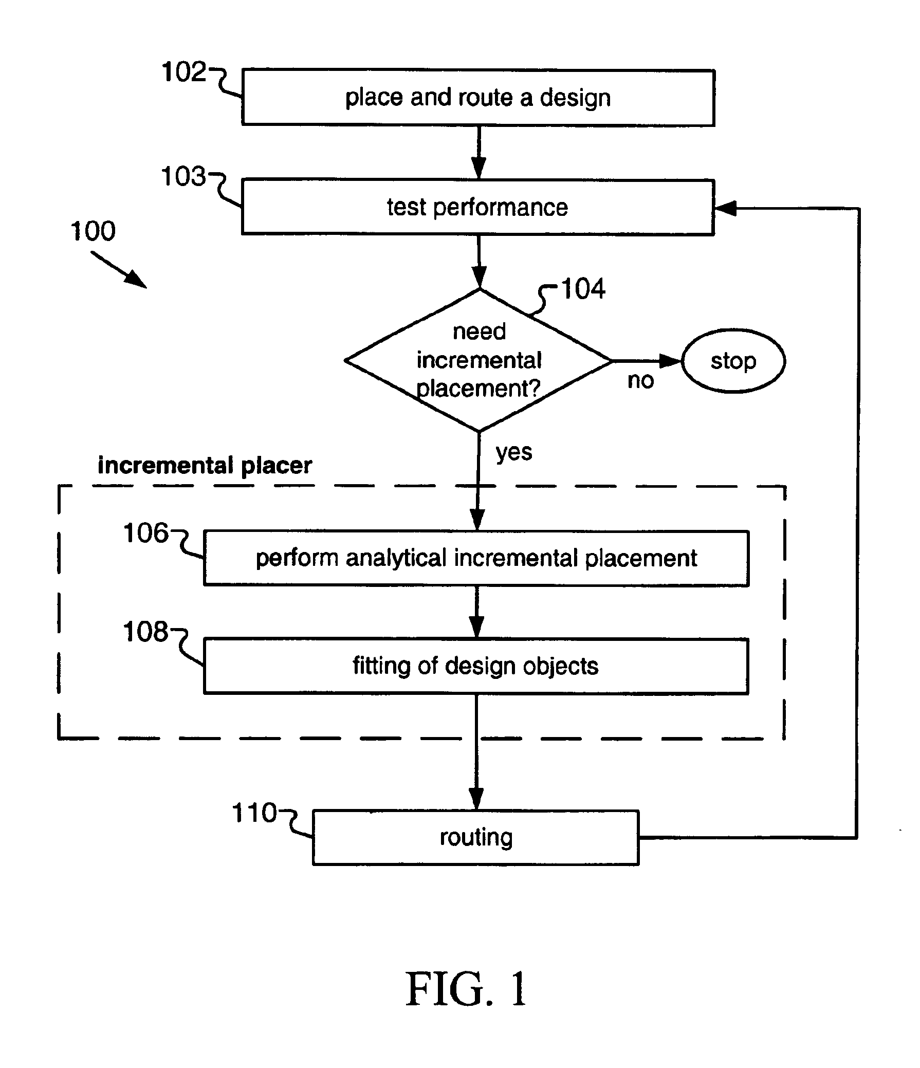
FIG. 1 is a flow chart 100 showing a CAD process that includes incremental placement of the present invention. In step 102, a design is placed and routed using conventional methods. In step 103, the performance of the design is tested using conventional timing analysis tools. In step 104, the performance is evaluated to determine if incremental placement is needed. If incremental placement is not needed, flow chart 100 terminates because there is no need to modify the layout. An example where incremental placement is n...


PUM


Abstract

An incremental placement method uses a set of connections to optimize and a set of movable design objects. The movable design objects are unplaced. A plurality of anchoring connections is associated with the movable design objects. A set of weights is associated with the set of connections to optimize and the plurality of anchoring connections. An objective function is constructed using the set of connections to optimize, the plurality of anchoring connections, and the set of weights. The objective function is minimized to obtain a placement of the movable design objects.

Description

FIELD OF THE INVENTIONThis invention relates to computer-aided design (CAD), and specifically, to placement of design objects in an integrated circuit.BACKGROUND OF THE INVENTIONThe design process for many integrated circuits (“chips”) typically contains a number of well known sequential operations. Initially, the proposed functionality of a circuit is analyzed by one or more chip designers. These designers then use design capture tools-to enter the logical components of the circuit and their interactions. This step involves generating a description of the logic design to be implemented on the circuit chip in an appropriate machine-readable form. One of the commonly used methods for specifying a design is a hardware description language (HDL). This language contains specific functions and syntax to allow complex hardware structures to be described in a compact and efficient way. Computer-aided design tools are available to compile the HDL description specifying the design into lower...

Claims


Application Information

Patent Timeline
IPC IPC(8): G06F17/50
CPCG06F17/5072G06F30/392
Inventor ANDERSON, JASON H.
Owner XILINX INC
Why Eureka
Try Eureka