Sample mount for a scanning electron microscope

a scanning electron microscope and sample mount technology, applied in the field of electron microscopes, can solve the problems of limited resolution at a level, high specialized equipment required, and conventional optical microscopes that are not suitable for wafer inspection, so as to prevent wafer inspection, increase inspection throughput, and quick and efficient edge mounting

Inactive Publication Date: 2005-03-29
MICRON TECH INC
View PDF6 Cites 5 Cited by
  • Summary
  • Abstract
  • Description
  • Claims
  • Application Information

AI Technical Summary

Benefits of technology

The present invention provides an improved sample mount that permits quick and efficient edge mounting of wafer samples within a SEM. Furthermore, mounting is accomplished without the use of messy adhesives and tapes. By avoiding the use of adhesives, the sample mount does not require the lengthy cure time often associated with adhesive mounts. Advantageously, inspection throughput is increased, preventing wafer inspection from becoming a production bottleneck.

Problems solved by technology

Due to the minute size of the wafer features, highly specialized equipment is required.
For various reasons, conventional optical microscopes are ill-fitted for wafer inspection.
For example, they are limited in their ability to resolve detail at a level sufficient to enable adequate wafer examination.
Additionally, they are unable to achieve the required magnification levels.
Furthermore, depth-of-field (i.e., the ability to keep objects at two different depths simultaneously in focus) is restricted, requiring the operator to constantly re-focus the microscope as different areas of the sample are inspected.
While such mounts have proven effective, drawbacks exist.
Additionally, the curable adhesive may require several hours to cure prior to inspection.
Thus, there are issues concerning increased setup time with current semiconductor sample retaining devices.

Method used


Image

  • Sample mount for a scanning electron microscope
  • Sample mount for a scanning electron microscope
  • Sample mount for a scanning electron microscope

Examples


Embodiment Construction

In the following detailed description of the embodiments, reference is made to the accompanying drawings which form a part hereof, and in which are shown by way of illustration specific embodiments in which the invention may be practiced. It is to be understood that other embodiments may be utilized and structural changes may be made without departing from the scope of the present invention.

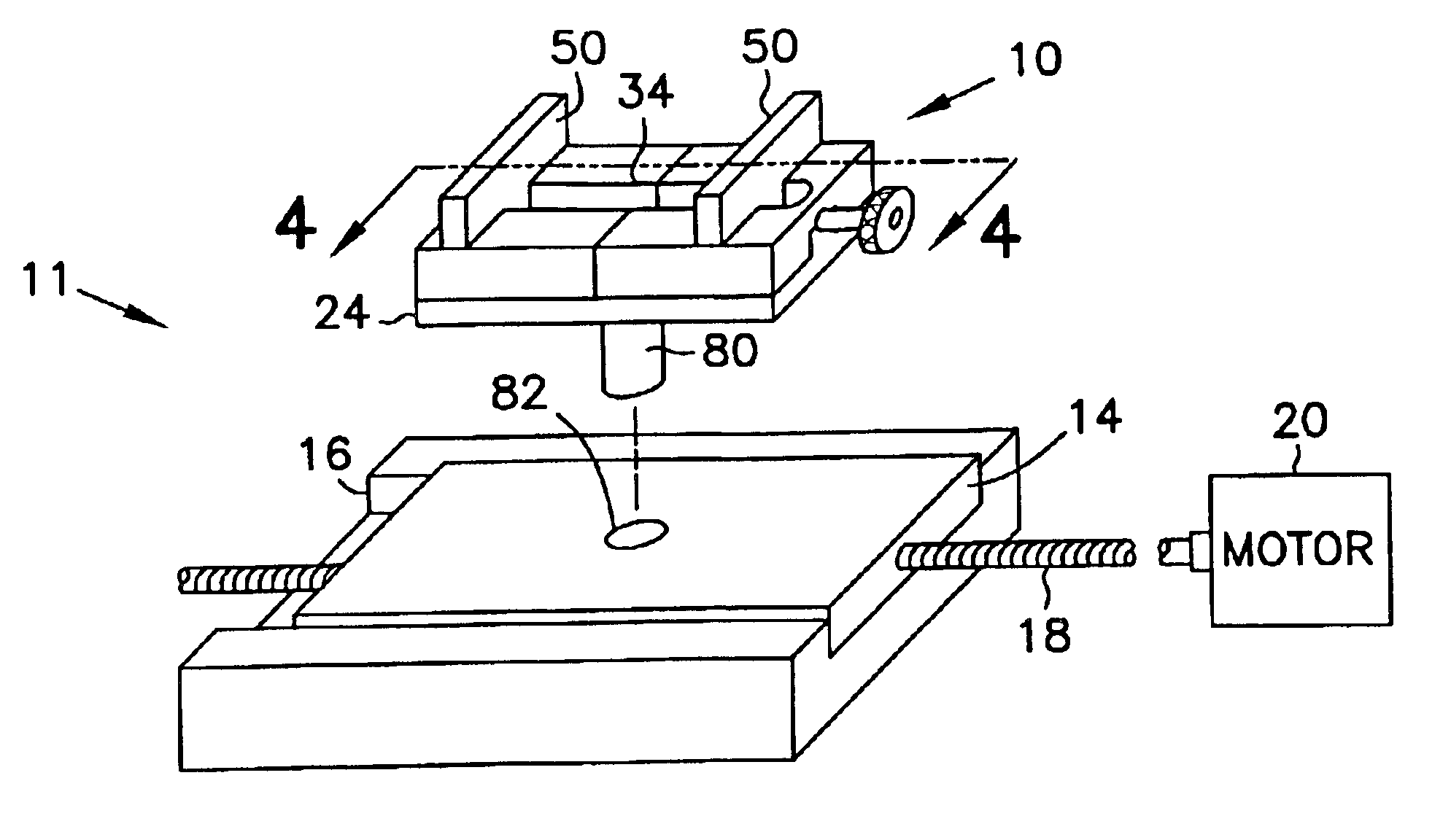
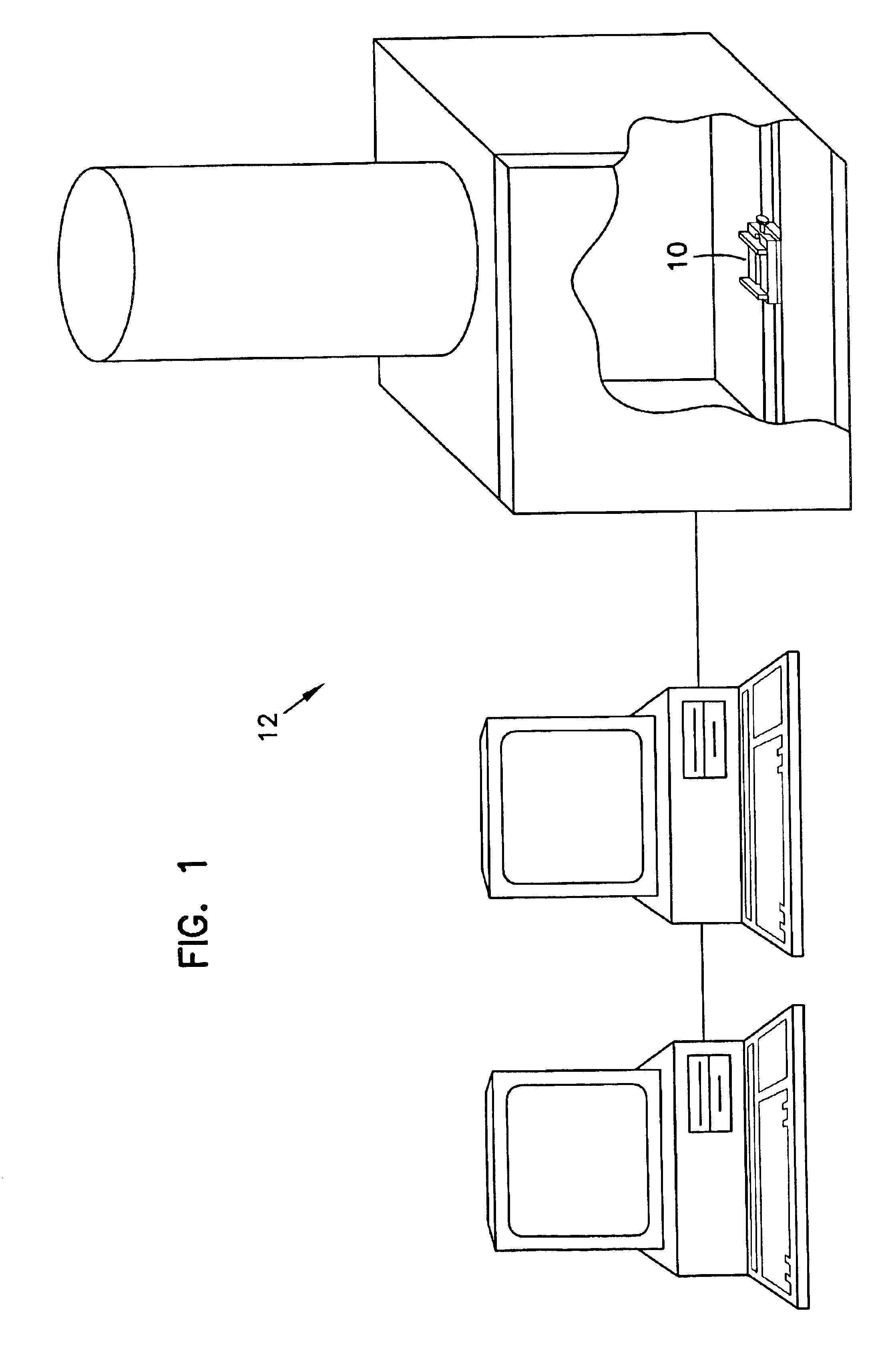
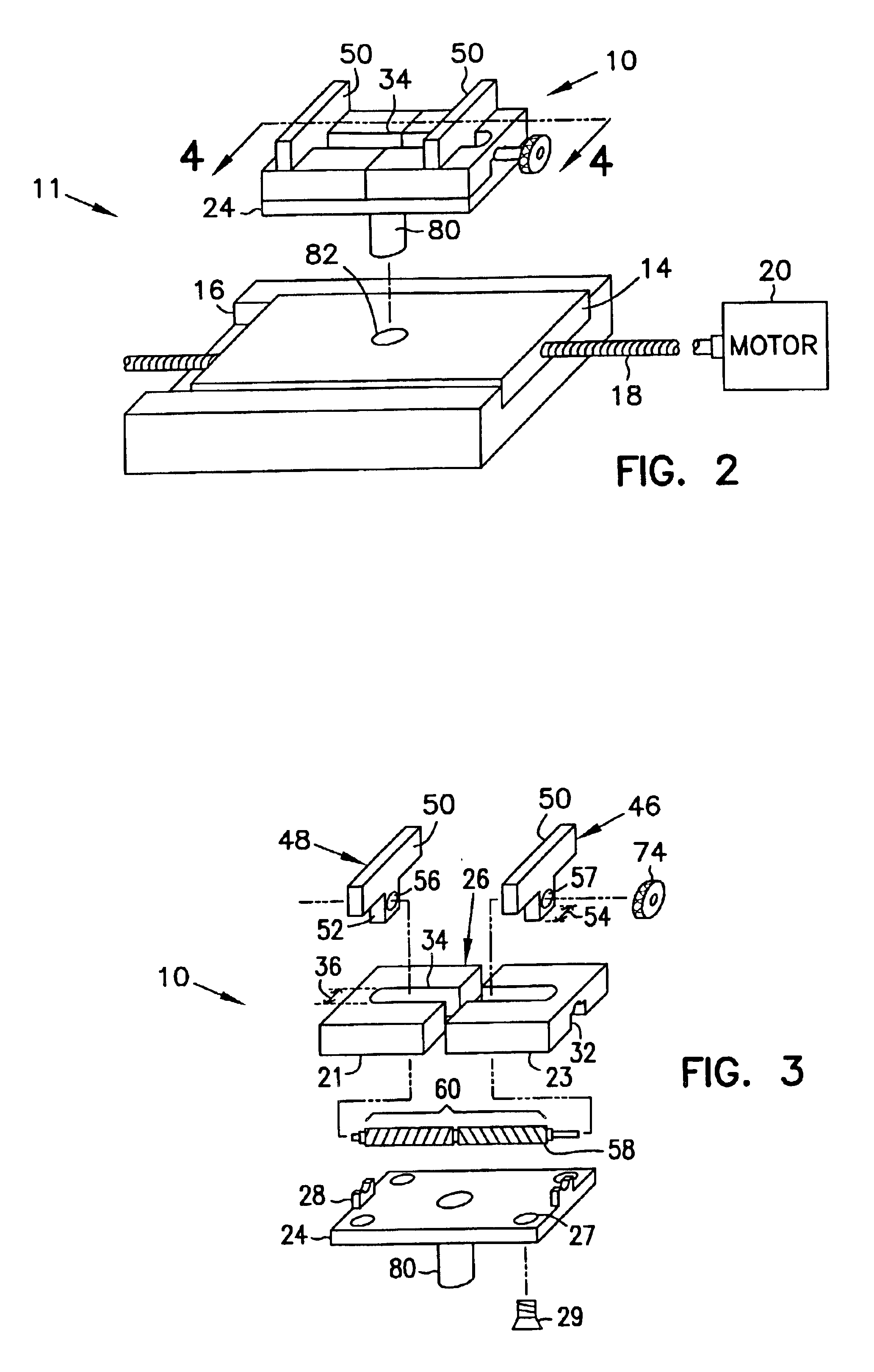
FIG. 1 shows a perspective view of one embodiment of a sample mount 10 in accordance with the present invention as it would be installed in a generic scanning electron microscope (SEM) 12. Referring to FIG. 2, a sample mounting assembly 11 includes the sample mount 10 and a base 14 to which the sample mount 10 is secured. The base 14 is positionable along a rail 16 and may be externally driven by a drive screw 18 operably connected to a drive motor 20. Alternatively, the base 14 may be manually positionable by a variety of devices known in the art or by hand. By selectively engaging the drive mot...


PUM


Abstract

A sample mount and method is disclosed for securing a semiconductor wafer sample to a generic base of a scanning electron microscope. The mount has two opposing clamp members that move relative to one another in response to rotational input to a lead screw. By placing a sample between the clamp members and rotating the lead screw, the samples may be clamped for inspection. When inspection is complete, the lead screw may be rotated in the opposite direction to release the clamping hold on the sample. The clamp members are adjustable to hold varying thicknesses and numbers of specimens making up the sample. In one embodiment, both clamp members move symmetrically from a common origin. In yet another embodiment, one clamp member is fixed relative to the mount and the other clamp member moves relative thereto.

Description

FIELD OF THE INVENTIONThe present invention pertains to electron microscopes. Specifically, this invention pertains to a sample mount for use with a scanning electron microscope.BACKGROUND OF THE INVENTIONThe semiconductor wafer fabrication process relies heavily on physical inspection processes to ensure product quality. Due to the minute size of the wafer features, highly specialized equipment is required. This equipment typically includes a variety of viewing instruments such as microscopes which permit a technician to accurately magnify and view specific features of the wafer sample.For various reasons, conventional optical microscopes are ill-fitted for wafer inspection. For example, they are limited in their ability to resolve detail at a level sufficient to enable adequate wafer examination. Additionally, they are unable to achieve the required magnification levels. Furthermore, depth-of-field (i.e., the ability to keep objects at two different depths simultaneously in focus)...

Claims


Application Information

Patent Timeline
Patent Type & Authority Patents(United States)
IPC IPC(8): H01J37/20
CPCH01J37/20
Inventor CARROLL, LYNN J.
Owner MICRON TECH INC
Why Eureka
Try Eureka