Plating apparatus for wafer

a technology of plating apparatus and wafer, which is applied in the direction of coating, electrolysis components, electrolysis processes, etc., can solve the problem of difficult to uniformly stir the whole region of plating solution

Inactive Publication Date: 2005-04-05
ELECTROPLATING ENGINEERS OF JAPAN LTD
View PDF9 Cites 25 Cited by
  • Summary
  • Abstract
  • Description
  • Claims
  • Application Information

AI Technical Summary

Benefits of technology

to provide a plating apparatus which enables the whole area of a target plating surface of a wafer to be subjected to more uniform plating treatment and moreover enables a target plating surface of a wider area to be subjected to positive and uniform plating treatment.

Problems solved by technology

And as described above, with this stirring means it is difficult to uniformly stir the whole region of plating solution.

Method used


Image

  • Plating apparatus for wafer
  • Plating apparatus for wafer
  • Plating apparatus for wafer

Examples


first embodiment

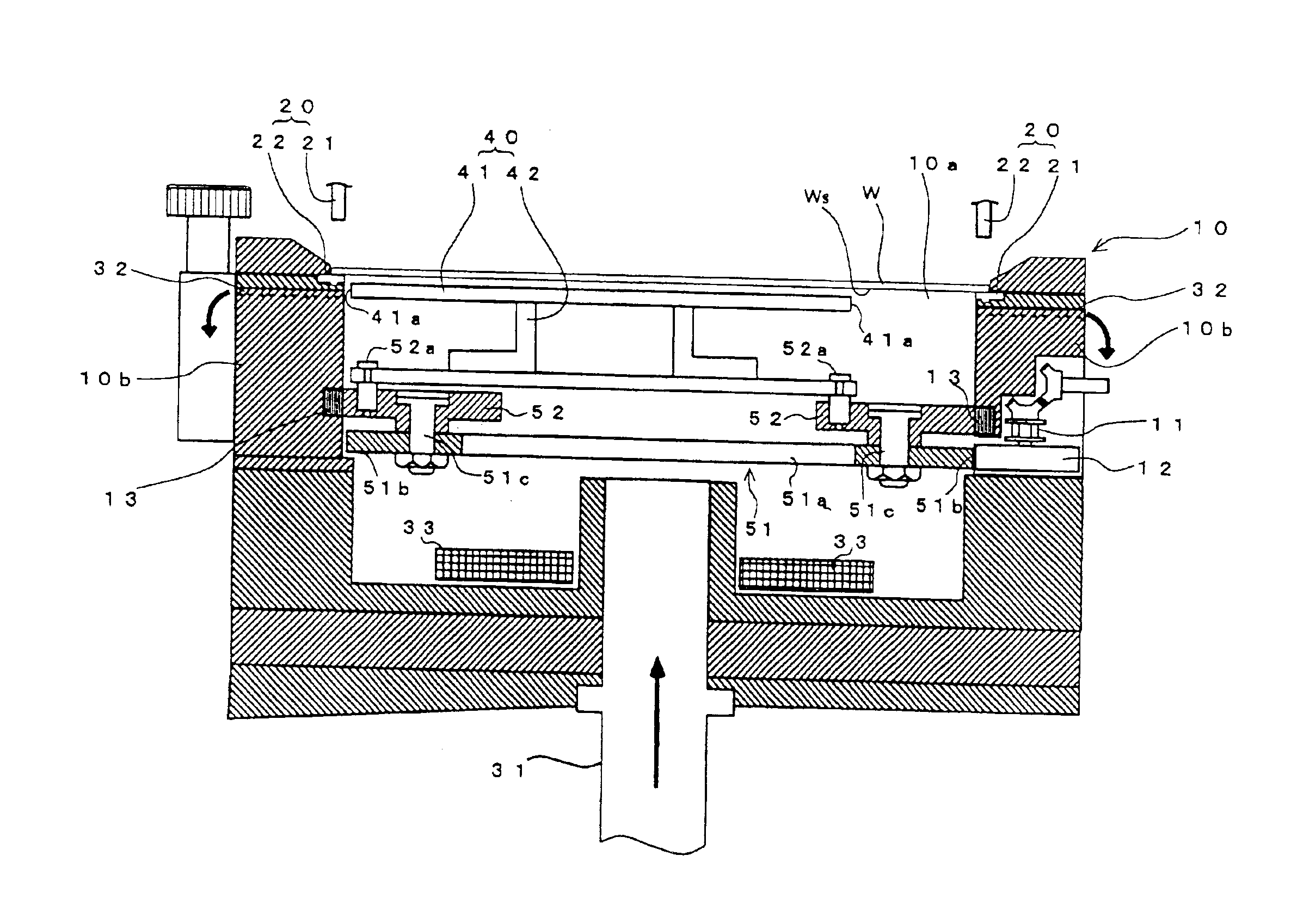
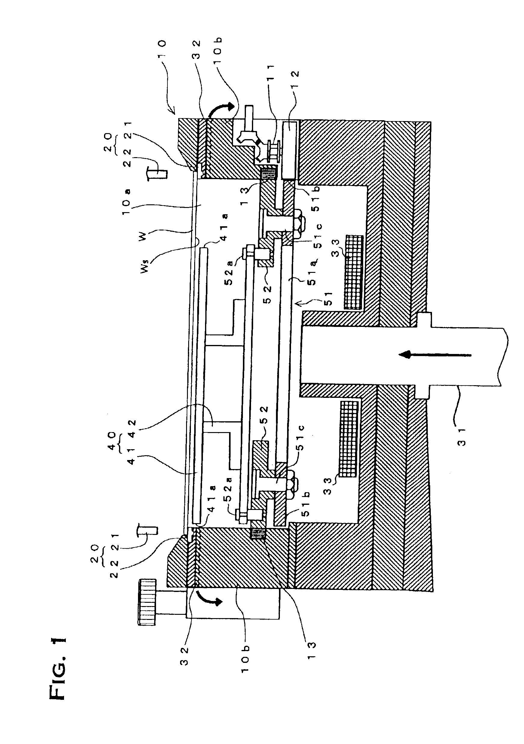
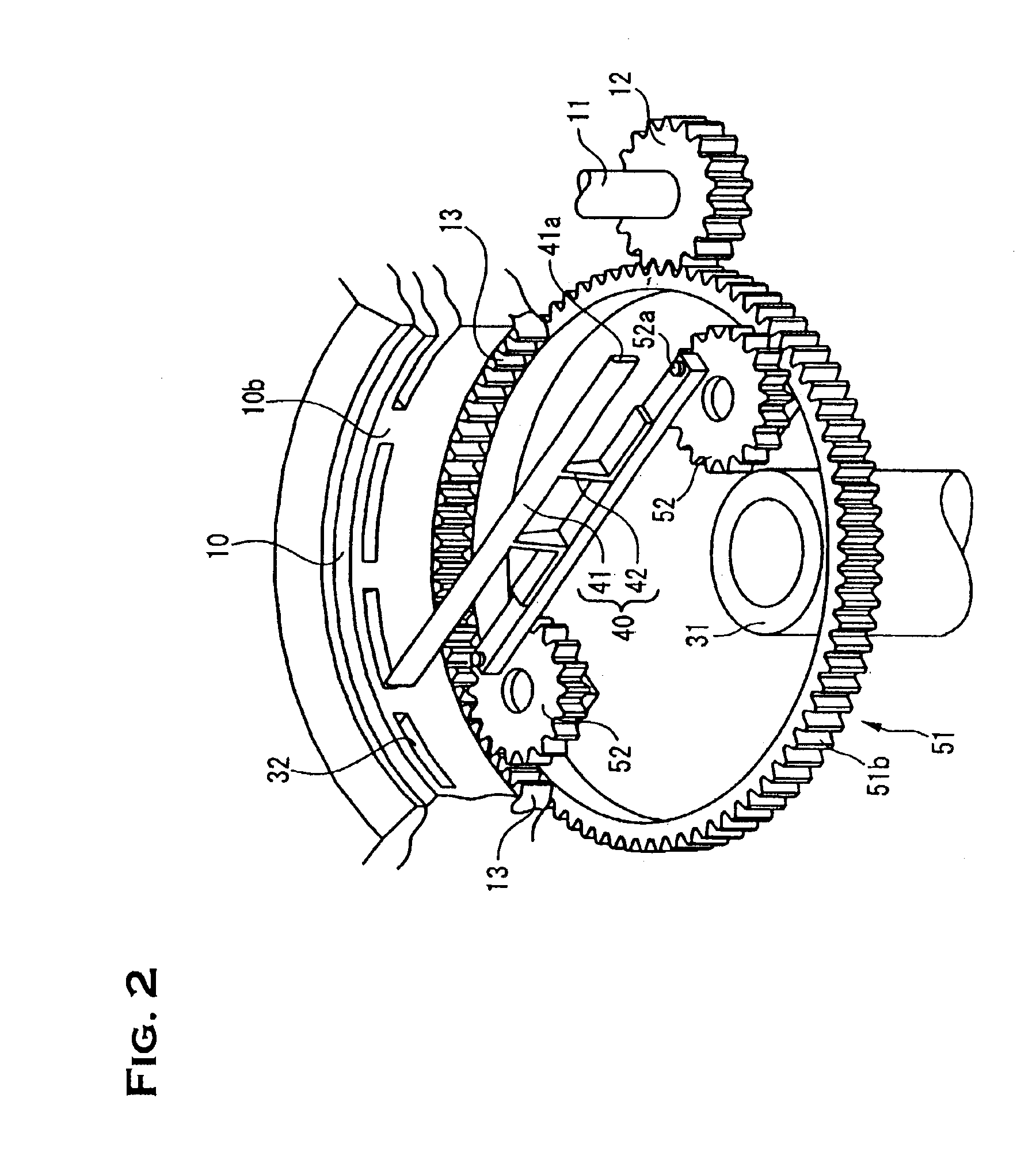
The plating apparatus for wafer shown in FIGS. 1 and 2 is a cup type plating apparatus. This plating apparatus is provided with a plating tank 10 which houses a plating solution, and the plating tank 10 has in its top portion an opening 10a on which a wafer W to be plated is placed. And a holding member (holding means) 20 which holds the wafer W is attached to the end edges of this opening 10a. Schematically, this holding member 20 is constituted by a seal packing 21 to prevent the leakage of the plating solution, a cathode electrode (a cathode) disposed on the packing 21, which is not shown, and a holder member 22 which holds the outer peripheral portion of the wafer W placed on the packing 21 from above along the whole circumference.

A supply pipe 31 for plating solution is connected to the bottom of the plating tank 10, and a discharge passage 32 of plating solution is formed above a side wall 10b of the plating tank 10, i.e., in a position adjoining to the holding member 20. The ...

second embodiment

Next, a description will be given below of a plating apparatus of the second embodiment in which the drive mechanism which rotates the external gear 51b is different from that of the first embodiment. Incidentally, because the basic construction of this plating apparatus is the same as that of the plating apparatus of the first embodiment, its description is omitted.

As shown in FIGS. 6(A) and 6(B), in this plating apparatus a driving shaft 11 which transmits rotations from a motor, which is not shown, (the driving side) and a driving gear 12 which meshes with an external gear 51b (the driven side) are connected together via a magnet coupling 60. Schematically, this magnet coupling 60, which is of a cylinder type, comprises an inner ring 61 to which the driving shaft 11 is connected (a driving side rotor), an outer ring 62 to which the driving shaft 12 is connected (a driven side rotor), and a partition wall 63 disposed between the inner ring 61 and the outer ring 62. The outer perip...

third embodiment

Next, a further embodiment in which a diaphragm is provided within the plating tank will be described below. Incidentally, because the basic construction of this plating apparatus is the same as that of the plating apparatus of the first embodiment, its description is omitted.

As shown in FIG. 7, the interior of the plating tank 10 of this plating apparatus is provided with a diaphragm 70 which partitions the interior of the plating tank 10 into an upper portion of the interior of the plating tank 10 in which a first stirrer 40 is installed (the cathode electrode side) and a lower portion of the interior of the plating tank 10 in which an anode electrode 33 is installed (the anode electrode side). The diaphragm 70 permits energization between the two electrodes through the plating solution (i.e., has energizing properties) and is made of, for example, woven fabrics of polypropylene filaments, ion exchange membranes including fluoroplastics-containing ion exchange membranes or non-wov...


PUM

PropertyMeasurementUnit
longitudinal sizeaaaaaaaaaa
radius sizeaaaaaaaaaa
driving forceaaaaaaaaaa

Abstract

A plating apparatus is provided to allow the whole area of a target plating surface of a wafer to be subjected to more uniform plating treatment and moreover enables a target plating surface of a wider area to be subjected to positive and uniform plating treatment. In the plating apparatus which has a stirring bar within a plating tank and which performs plating treatment of a target plating surface of the wafer while stirring a plating solution near the target plating surface of the wafer by moving the stirring bar, the stirring bar is rotated while being oscillated in a motion plane substantially parallel to the target plating surface of the wafer. By this operation, the occurrence of an eddy flow of the plating solution is suppressed during stirring and it becomes possible to positively carry out more uniform plating treatment of a wider region.

Description

BACKGROUND OF THE INVENTION1. Field of the InventionThe present invention relates to a plating apparatus of semiconductor wafer and, more particularly, to a plating apparatus of semiconductor wafer comprising stirring means for a plating solution within a plating tank.2. Description of the Related ArtAs a type of plating apparatus of semiconductor wafer there is available what is called a cup type plating apparatus. The cup type plating apparatus comprises a plating tank, which has an opening in its top part, and a wafer support portion provided along the opening. And the plating tank comprises a solution supply pipe connected to the bottom of the tank as means for circulating a plating solution and a solution discharge passage formed on a side surface of the plating tank in a position near the top opening. The plating solution is supplied from the solution supply pipe to the interior of the plating tank and discharged from the solution discharge passage to outside the plating tank....

Claims


Application Information

Patent Timeline
Patent Type & Authority Patents(United States)
IPC IPC(8): C25D7/12
CPCC25D17/001
Inventor SAKAKI, YASUHIKO
Owner ELECTROPLATING ENGINEERS OF JAPAN LTD
Why Eureka
Try Eureka