Fabrication of an EEPROM cell with emitter-polysilicon source/drain regions

a polysilicon source/drain and eeprom cell technology, applied in the direction of semiconductor devices, electrical apparatus, transistors, etc., can solve the problems of no simple and economical way to integrate these two device types into a single integrated circuit, and achieve the effect of increasing the breakdown voltage of the eeprom well and increasing the breakdown voltag

a polysilicon source/drain and eeprom cell technology, applied in the direction of semiconductor devices, electrical apparatus, transistors, etc., can solve the problems of no simple and economical way to integrate these two device types into a single integrated circuit, and achieve the effect of increasing the breakdown voltage of the eeprom well and increasing the breakdown voltag

US6875648B1Active Publication Date: 2005-04-05ATMEL CORP

Image

  • Fabrication of an EEPROM cell with emitter-polysilicon source/drain regions
  • Fabrication of an EEPROM cell with emitter-polysilicon source/drain regions
  • Fabrication of an EEPROM cell with emitter-polysilicon source/drain regions

Examples


Embodiment Construction

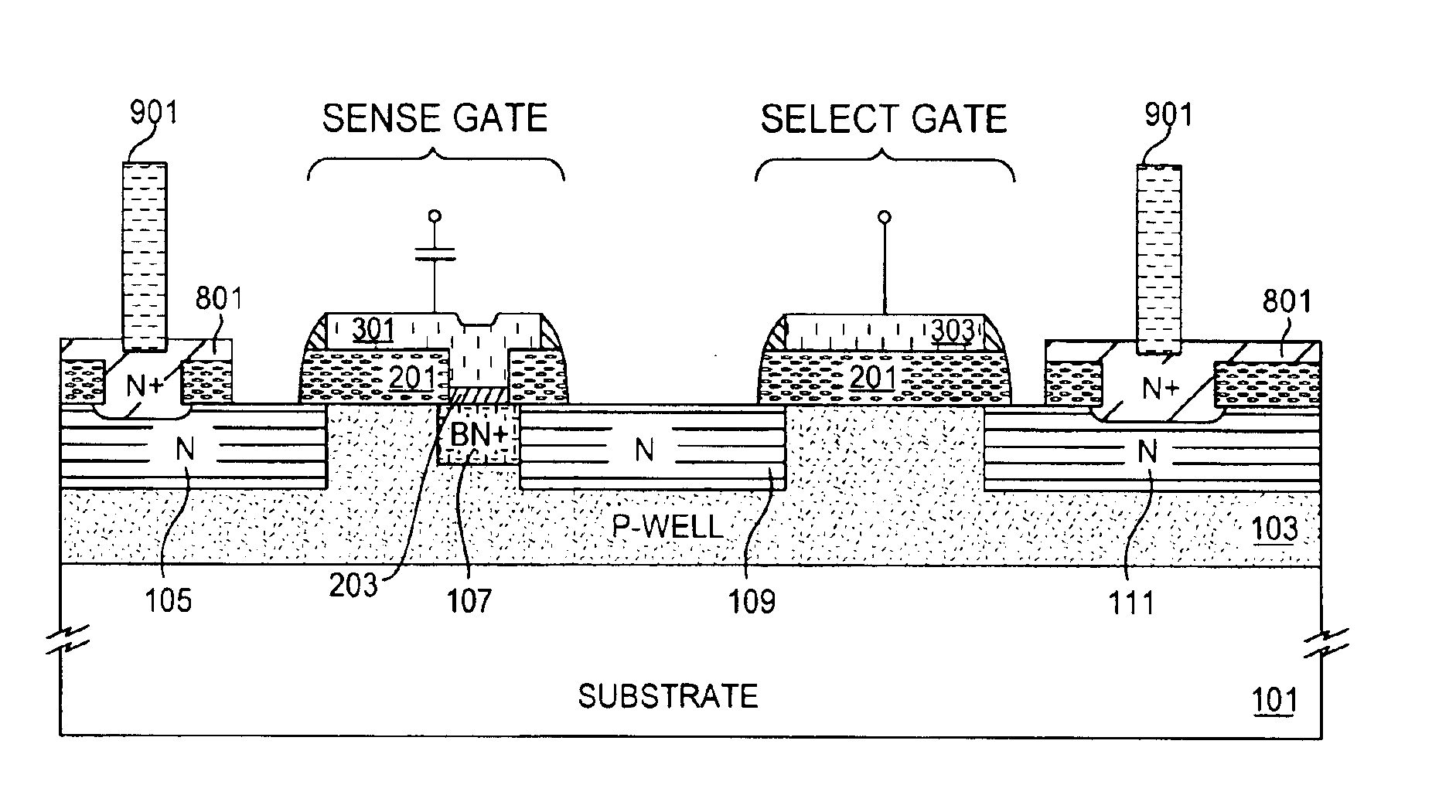
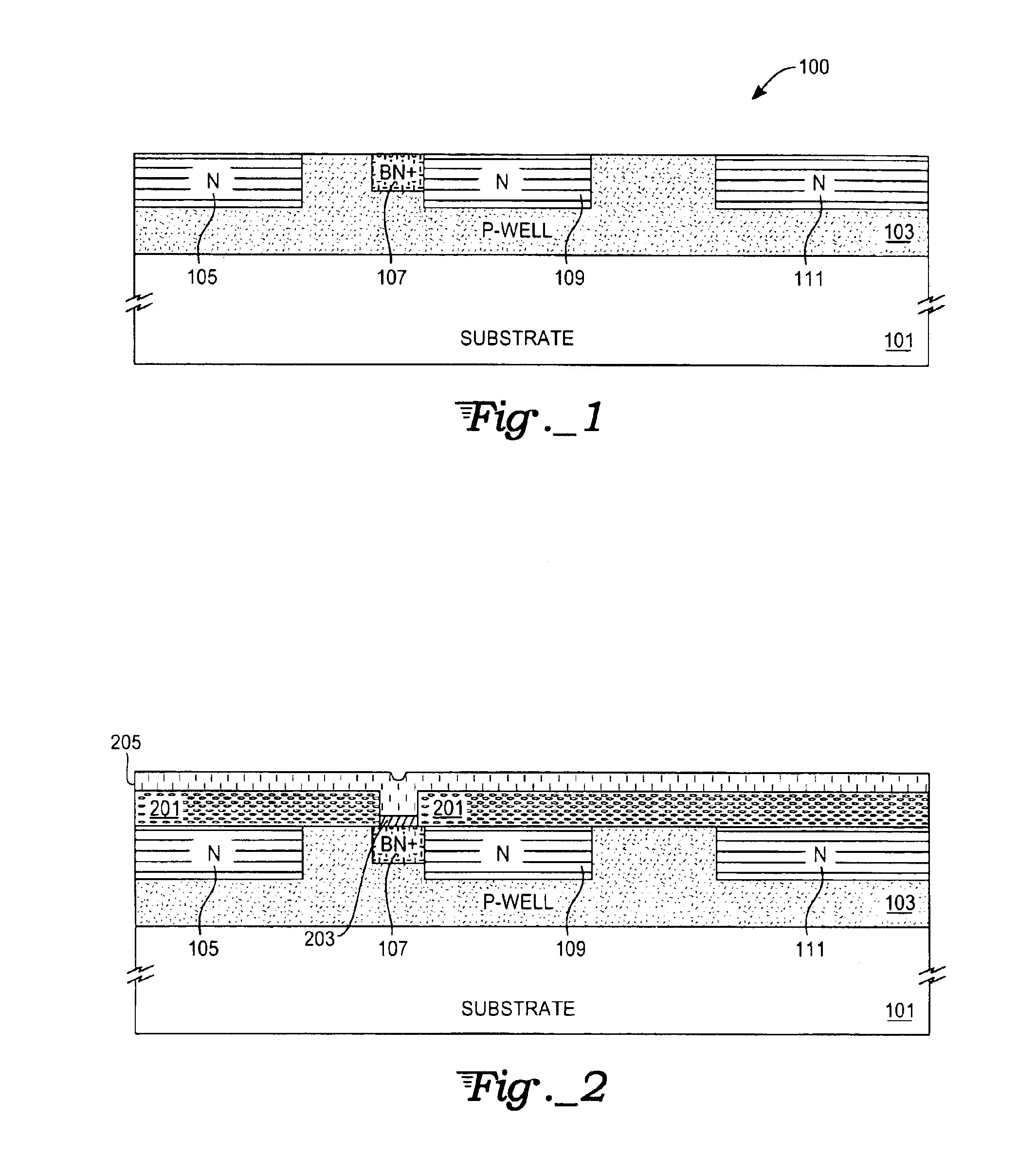
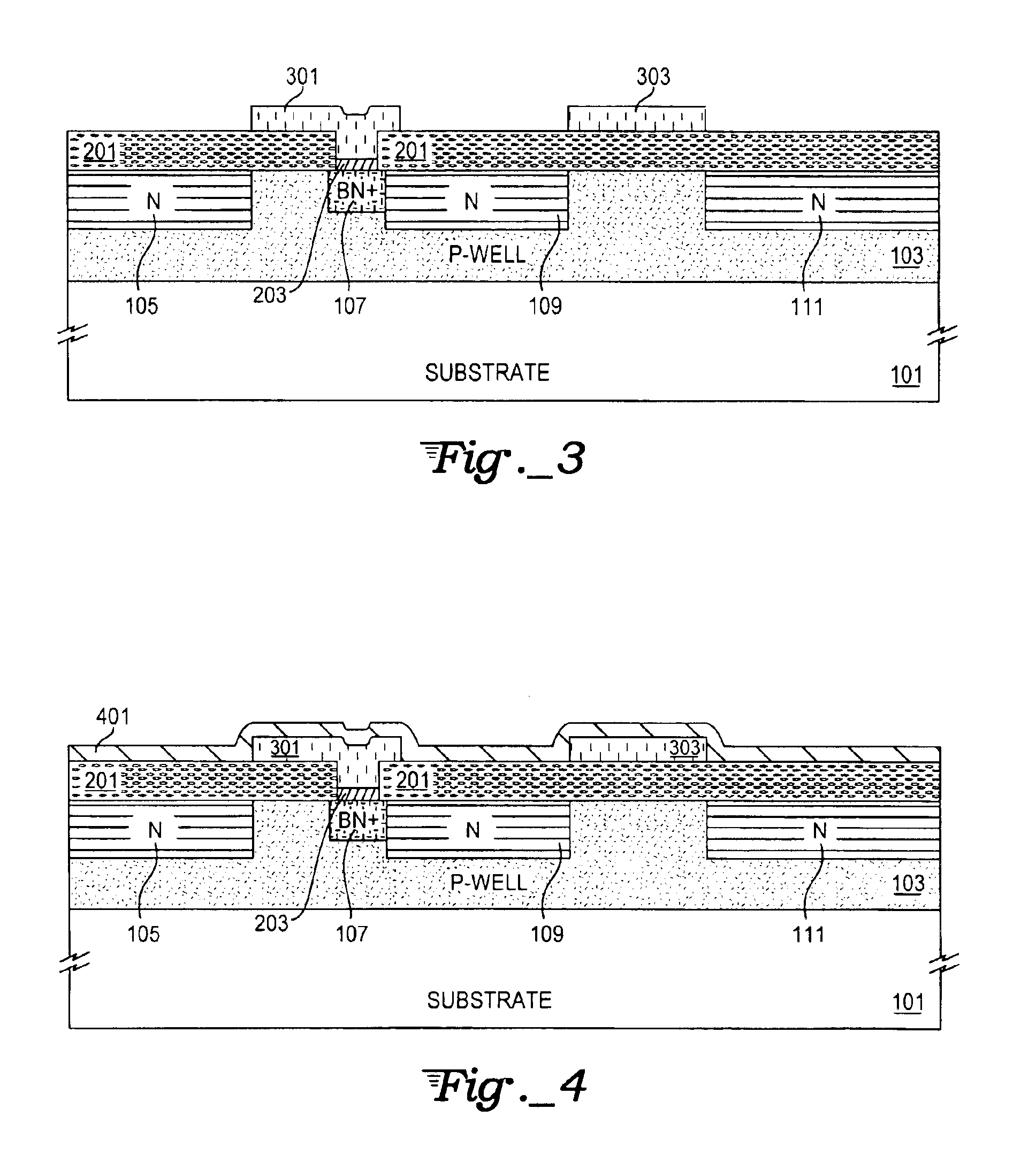
An electronic memory device of the present invention has source / drain junctions with a relatively high breakdown voltage (e.g., about 14 volts or approximately 12-15 volts). The breakdown voltage of MOS devices on a typical BiCMOS process is only about 10 volts. A lower well breakdown voltage is attributed to a deep (e.g., approximately 200 nm or greater (0.2 μm)) source / drain doped region. Using an emitter polysilicon film of the present invention to fabricate source / drain regions of an MOS device results in shallow junctions (i.e., less than 0.1 μm) and a resulting higher breakdown voltage. Therefore, the high breakdown voltage allows the present invention to be fabricated in an integrated CMOS / Bipolar (i.e., BiCMOS) line, allowing CMOS, bipolar devices (e.g., an NPN transistor), and EEPROMs to be formed in an integrated circuit.

With reference to FIGS. 1-9, an exemplary embodiment of the present invention is described according to the following process steps. FIG. 1 includes a cro...


PUM


Abstract

An EEPROM memory cell uses an emitter polysilicon film for fabricating shallow source / drain regions to increase a breakdown voltage of the wells. The wells are fabricated to be approximately 100 nm (0.1 micrometers (μm)) in depth with a breakdown voltage of approximately 14 volts or more. A typical breakdown voltage of a well in a bipolar process is approximately 10 volts. Due to the increased breakdown voltage achieved, EEPROM memory cells can be produced along with bipolar devices on a single integrated circuit chip and fabricated on a common semiconductor fabrication line.

Description

TECHNICAL FIELDA present invention described herein relates generally to a process for fabricating an integrated circuit structure, and more specifically to an electronic memory device and a process for manufacture.BACKGROUND ARTSemiconductor memory devices are typically classified into volatile memory devices and non-volatile memory devices. Volatile memory devices are subdivided into dynamic random-access memories (DRAMs) and static random access memories (SRAMs). Non-volatile memory types include erasable programmable read-only memories (EPROMS) and electrically erasable programmable read-only memories (EEPROMs). EEPROMs are increasingly used in system programming that requires continuous update or auxiliary memory devices. Particularly, flash EEPROMs are advantageous as mass storage devices because their integration density is high compared with conventional EEPROMs.Frequently, it would be convenient to be able to mix integrated circuit device types, such as EEPROMs and other me...

Claims


Application Information

Patent Timeline
05 Apr 2005
Publication
US6875648B1
IPC
H01L21/70; H01L21/8238; H10B69/00; H10B99/00
CPC
H01L21/823425; H01L21/8249; H01L27/0623; H01L27/1052; H01L27/115; H01L27/105; H01L27/11558; H10B41/60
Inventors
CHAUDHRY, MUHAMMAD I.