Field-effect organic transistor

a field-effect organic transistor and transistor technology, applied in transistors, solid-state devices, thermoelectric devices, etc., can solve the problems of low mobility of organic semiconductors, low threshold voltage, fluctuation of threshold voltage, etc., and achieve low threshold voltage and high mobility.

Inactive Publication Date: 2005-04-05
CANON KK
View PDF4 Cites 32 Cited by
  • Summary
  • Abstract
  • Description
  • Claims
  • Application Information

AI Technical Summary

Benefits of technology

The present invention can provide a field-effect organic transistor having a high mobility and a low threshold voltage and small fluctuate of a threshold voltage, and useful for electronic devices, e.g., displays, information tags and ICs.

Problems solved by technology

However, the organic semiconductors proposed so far have a disadvantage of a low mobility, limited to the order of 10−1 cm2 / Vs for production by vacuum evaporation process, and 10−2 cm2 / Vs for production by a liquid-phase process.
Other problems involved in organic transistors are a high threshold voltage and fluctuation of a threshold voltage in driving for a long period.
Few organic transistors have been commercialized because of these problems.

Method used


Image

  • Field-effect organic transistor
  • Field-effect organic transistor
  • Field-effect organic transistor

Examples


example 1

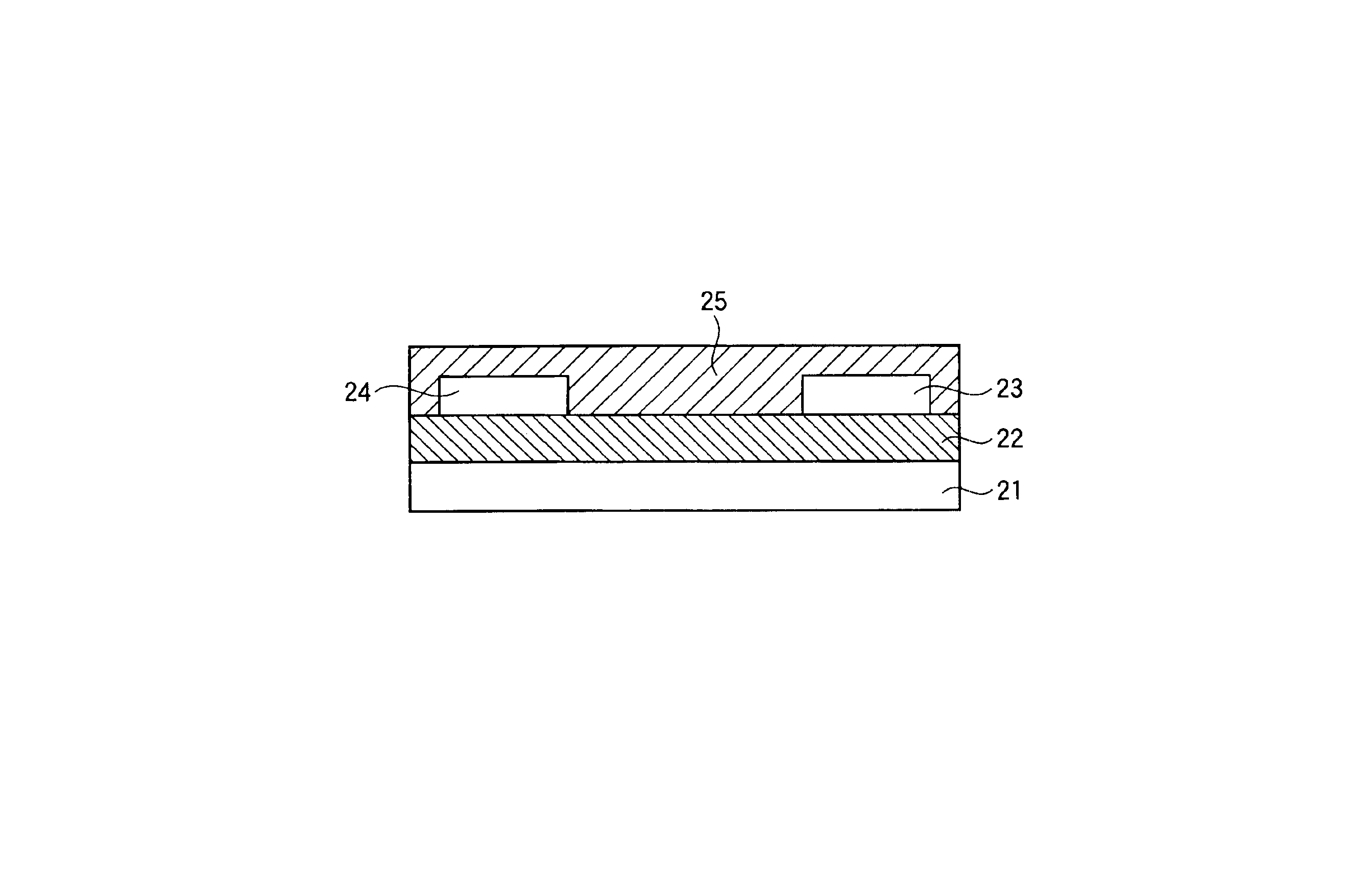
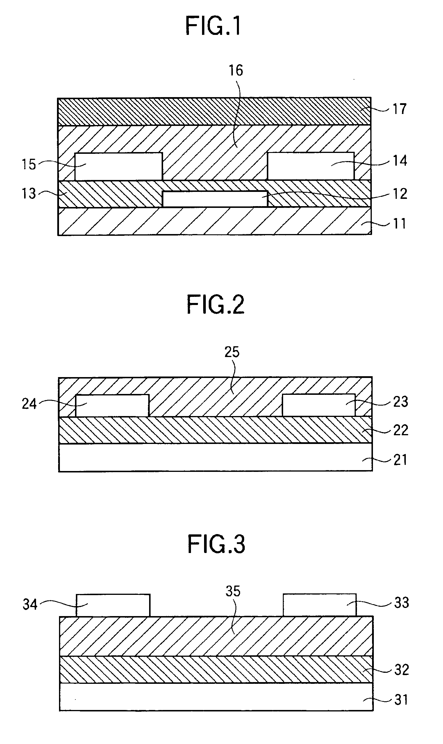
FIG. 2 shows a structure of the field-effect organic transistor prepared in Example 1.

As the gate electrode 21, an n-type, highly-doped silicon substrate was used; as the gate insulating layer 22, SiO2 was used; as the source electrode 23 and the drain electrode 24, a chromium / gold stack was used; and as the organic semiconductor layer 25, the condensed aromatic ring compound A represented by the following chemical formula.

The procedure for forming the field-effect organic transistor is described below.

On the silicon substrate, a 300 nm thick, thermally oxidized film SiO2 was formed. The source and drain electrodes of chromium (thickness: 5 nm) / gold (thickness: 100 nm) having a channel length of 50 μm and a channel width of 50 mm were formed thereon by the lift-off method. The organic semiconductor layer 25 was formed by sublimating the condensed aromatic ring compound A in a metal sublimating boat being 10 cm apart from the substrate, at 5×10⁻⁶ torr at an average sublimation rate ...

example 2

The field-effect organic transistor having the same structure as the one prepared in Example 1 as shown in FIG. 2 was prepared using an n-type, highly-doped silicon substrate as the gate electrode 21, SiO2 as the gate insulating layer 22, the chromium / gold stack as the source electrode 23 and the drain electrode 24, and the condensed aromatic ring compound C represented by the following chemical formula as the organic semiconductor layer 25.

The procedure for forming the field-effect organic transistor is described below.

On the silicon substrate 21, a 300 nm thick, thermally oxidized film SiO2 was formed. The source and drain electrodes of chromium (thickness: 5 nm) / gold (thickness: 100 nm) having a channel length of 50 μm and a channel width of 50 mm were formed thereon by the lift-off method. The organic semiconductor layer 25 was formed thereon by applying a 0.01 g / mL chloroform solution of the condensed aromatic ring compound C by spin coating, and drying at 150° C. for 12 hours...

example 3

The field-effect organic transistor having the same structure as prepared in Example 2, as shown in FIG. 2 was prepared using an n-type, highly-doped silicon substrate as the gate electrode 21, polyvinyl phenol as the gate-insulating layer 22, gold as the source electrode 23 and the drain electrode 24, and the condensed aromatic ring compound C as the organic semiconductor layer 25.

The procedure for forming the field-effect organic transistor is described below.

2-propanol solution of polyvinyl phenol (0.1 g / mL) was applied by spin coating on the silicon substrate and dried at 150° C. for 6 hours to form a gate insulating layer. Thereon, gold (50 nm) was deposited by vacuum evaporation to produce source and drain electrodes with a channel length of 50 μm and a channel width of 10 mm. Thereon, chloroform solution of the condensed aromatic ring compound C (0.01 g / ml) was applied by spin coating and dried at 150° C. for 12 hours to form an organic semiconductor layer 25. The gate electr...


PUM

PropertyMeasurementUnit
energy band gapaaaaaaaaaa
channel widthaaaaaaaaaa
channel lengthaaaaaaaaaa

Abstract

It is an object of the present invention to solve the problems of the conventional organic transistors, such as a low mobility, a high threshold voltage and fluctuation of a threshold voltage in driving for a long period. The field-effect organic transistor of the present invention comprises 3 electrodes being source, drain and gate electrodes, a gate insulating layer and an organic semiconductor layer, wherein the organic semiconductor layer contains an organic semiconductor having 2 or more repeating units, each of the repeating units having a condensed aromatic ring compound having 10 or more conjugate double bonds and 3 two-fold axes.

Description

BACKGROUND OF THE INVENTION1. Field of the InventionThe present invention relates to a field-effect organic transistor, more specifically a field-effect organic transistor useful for the electronic devices, e.g., displays, information tags and ICs.2. Related Background ArtAn organic transistor which utilizes an organic semiconductor can be formed on a plastic substrate and into a large picture plane, while a silicon transistor has difficulty in this regard, and has been increasingly expected to apply to new devices, e.g., flexible electronic paper and information tags.An organic semiconductor produced by a vacuum evaporation process is disclosed by Japanese Patent Application Laid-Open No. 2001-094107, and an organic semiconductor produced by a liquid-phase process is disclosed by U.S. Pat. No. 6,107,117.However, the organic semiconductors proposed so far have a disadvantage of a low mobility, limited to the order of 10−1 cm2 / Vs for production by vacuum evaporation process, and 10−2...

Claims


Application Information

Patent Timeline
Patent Type & Authority Patents(United States)
IPC IPC(8): H01L51/05H01L51/30H01L29/786H01L51/00
CPCH01L51/0044H01L51/0052H01L51/0058H01L51/0077H01L51/0056H01L51/0053H01L51/0545H10K85/154H10K85/621H10K85/624H10K85/615H10K85/626H10K85/30H10K10/466
Inventor NAKAMURA, SHINICHI
Owner CANON KK
Why Eureka
Try Eureka