Etch stop for copper damascene process

Inactive Publication Date: 2005-04-05
CHARTERED SEMICONDUCTOR MANUFACTURING
View PDF6 Cites 1 Cited by
  • Summary
  • Abstract
  • Description
  • Claims
  • Application Information

AI Technical Summary

Benefits of technology

Another object of the present invention has been to provide an etch stop layer that simplifies the formation of said copper connectors.
A further object of the present invention has been to provide means for preventing the outdiffusion of copper from said connector into adjoining layers.
Yet another object of the present invention has been to provide a method for manufacturing said copper connector that achieves the above objects simultaneously in an efficient manner.
These objects have been achieved by providing a dual damascene copper connector whose upper surface is coplanar with the upper surface of the insulating layer in which it is embedded. Out-diffusion of copper from the connector is preven

Problems solved by technology

Thus, in this regard, aluminum, which has been the material of choice since the integrated circuit art began, is becoming less attractive than other better conductors such as copper, gold, and silver.
The metals in question have not been widely used for wiring as yet because they also suffer from a number of disadvantages, including formation of undesirable intermetallic alloys and/or recombination centers in other parts of the integrated circuit and they often have high diffusion rates.
Copper has the additiona

Method used


Image

  • Etch stop for copper damascene process
  • Etch stop for copper damascene process
  • Etch stop for copper damascene process

Examples


Example

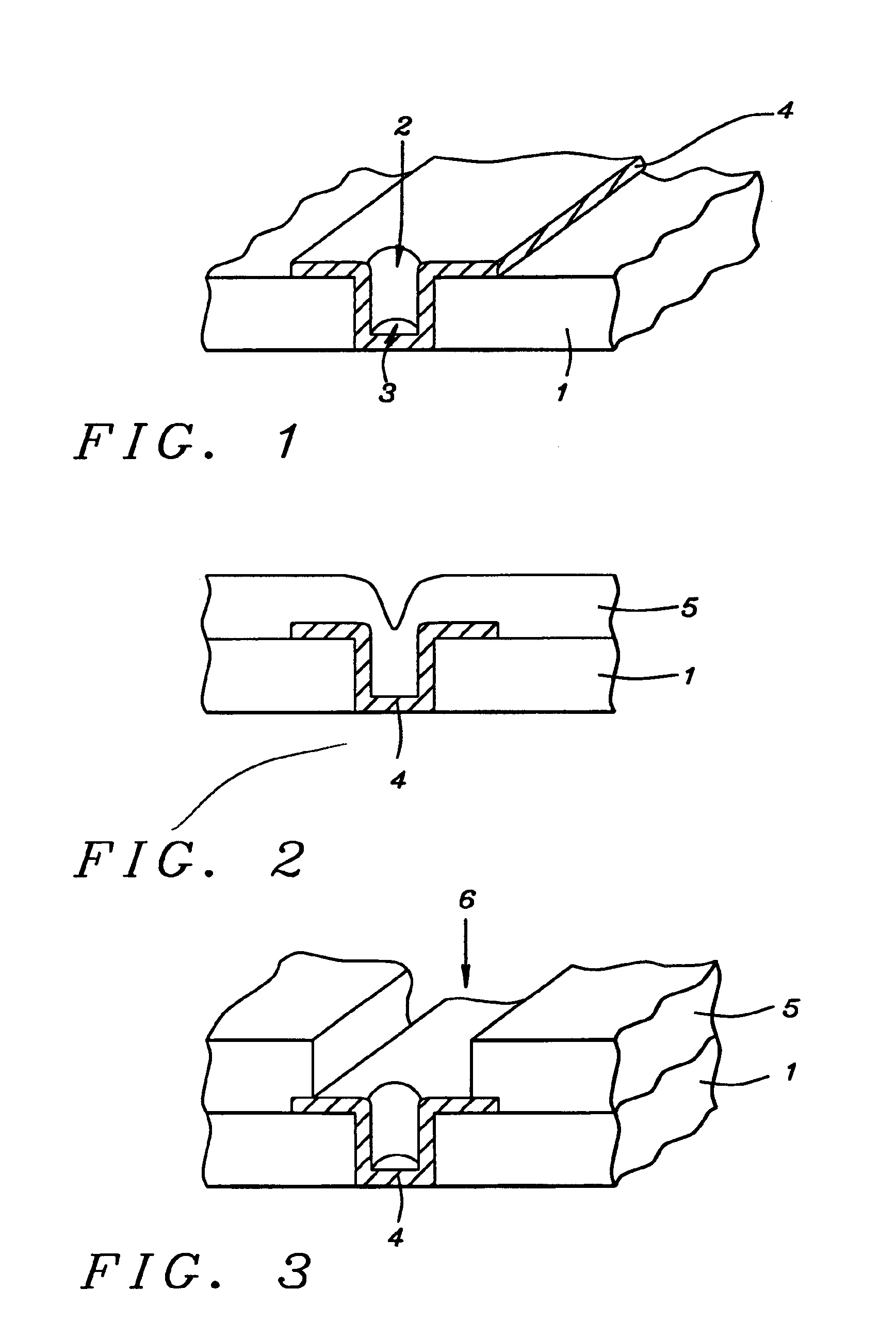
Referring now to FIG. 1 we begin a description of the dual damascene process. Insulating layer 1 has been deposited onto the upper surface of a partially completed integrated circuit (not shown). Cavity 2 has been etched all the way through layer 1. It is shown as cylindrical in cross-section, but any shape (such as rectangular) could be used. Barrier layer 4 has been deposited to line the walls of cavity 3 and has also been extended outwards from the rim of the cavity for some distance along the top surface of 1.

Insulating layer 5 is then deposited over the structure (as shown in FIG. 2) following which trench 6 is formed by etching all the way through layer 5. Trench 6 is narrower than the extension of barrier layer 4. This allows etching to proceed until cavity 2 has been re-formed without any danger of the etchant attacking layer 1 since layer 4 acts as an etch stop. This is illustrated in FIG. 3.

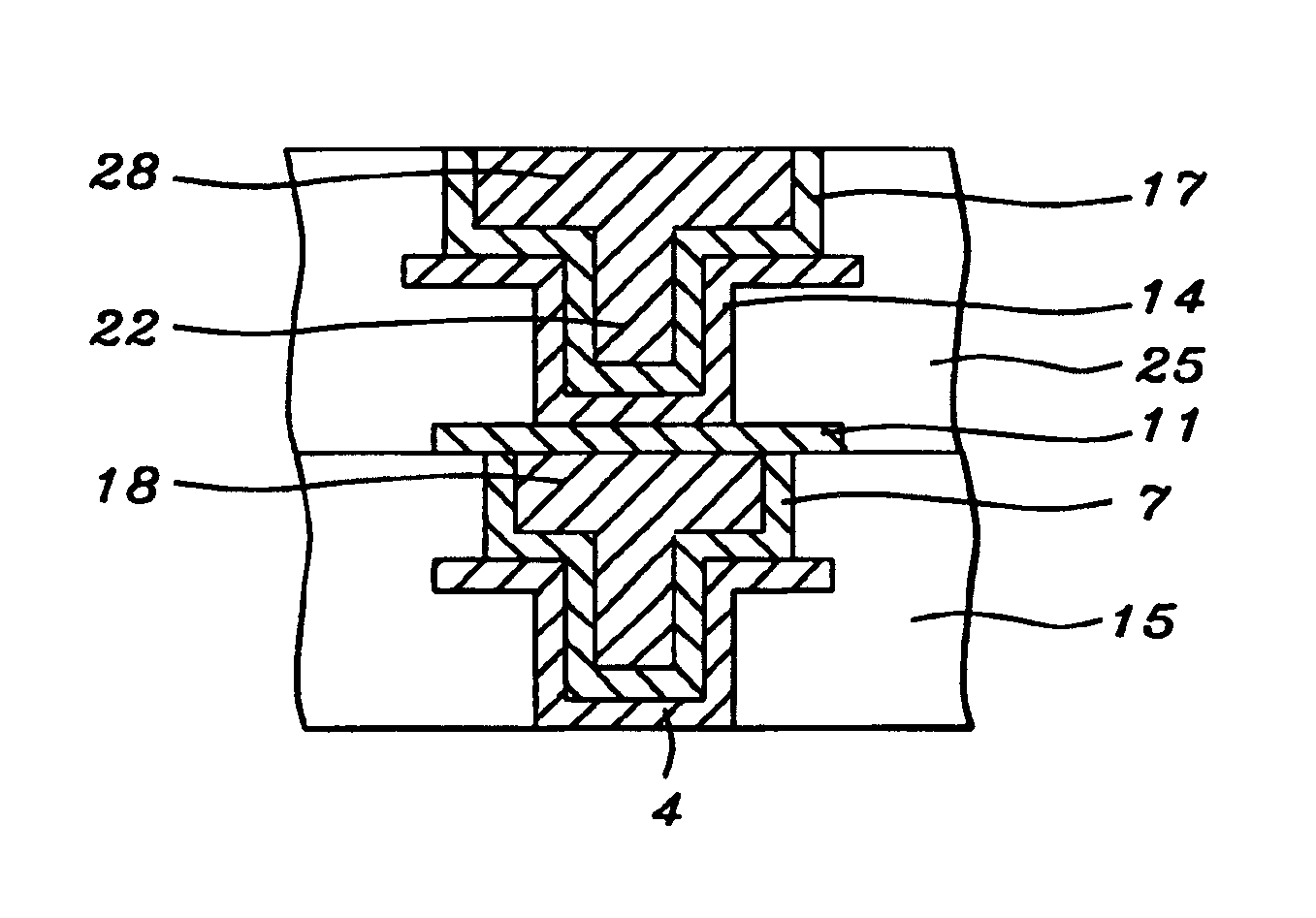
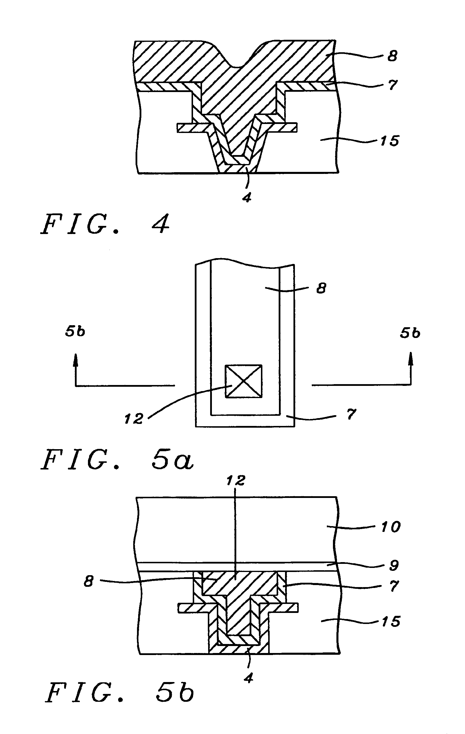
Referring now to FIG. 4, a second barrier layer 7 is deposited so as to coat the wa...


PUM


Abstract

The invention describes the application of copper damascene connectors to a double level metal process. A dual damascene copper connector whose upper surface is coplanar with the upper surface of the insulating layer in which it is embedded is described. Out-diffusion of copper from the connector is prevented by at least two barrier layers. One or two barrier layers are located at the interface between the connector and the insulating layer while another barrier layer comprises conductive material and covers the upper surface of the connector. When a second damascene connector is formed above the first connector the conductive barrier layer facilitates good contact between the two connectors. It also acts as an etch stop layer during the formation of the second connector. A process for manufacturing this structure is also described. It involves over-filling a trench in the surface of the insulator with copper and then removing the excess by chem.-mech. polishing.

Description

BACKGROUND OF THE INVENTION(1) Field of the InventionThe invention relates to the general field of integrated circuits, more particularly to the formation of copper interconnections therein.(2) Description of the Prior ArtAs wire widths in integrated circuits continue to shrink, the electrical conductivity of the wiring material itself becomes increasingly more important. Thus, in this regard, aluminum, which has been the material of choice since the integrated circuit art began, is becoming less attractive than other better conductors such as copper, gold, and silver. These materials, in addition to their superior electrical conductivity, are also more resistant than aluminum to electromigration, a quality that grows in importance as wire widths decrease.The metals in question have not been widely used for wiring as yet because they also suffer from a number of disadvantages, including formation of undesirable intermetallic alloys and / or recombination centers in other parts of the ...

Claims


Application Information

Patent Timeline
IPC IPC(8): G11B23/00G11B17/02H01L21/768
CPCG11B17/02G11B23/0021H01L21/76808H01L2221/1031H01L2924/0002H01L2924/00
Inventor TEONG, SU-PING
Owner CHARTERED SEMICONDUCTOR MANUFACTURING
Why Eureka
Try Eureka