Interlaced alternating pixel design for high sensitivity CMOS Image sensors

Inactive Publication Date: 2005-04-05
ALCOR MICRO CORP
View PDF7 Cites 17 Cited by
  • Summary
  • Abstract
  • Description
  • Claims
  • Application Information

AI Technical Summary

Benefits of technology

Therefore, one advantage of the present invention is to significantly reduce the size and manufacturing cost of the CMOS sensor by a special pixel design arrangement, while still maintaining or even enhancing

Problems solved by technology

Integrated circuit chips containing CCD image sensors are expensive because of the specific A manufacture process required.
The CCD also requires relatively large power dissipation, because of the required clock signals and the high voltage that is usually needed.
However, it is well known that the CMOS image sensor suffers from noises which will adversely degrade the performance.
These noises include kTC noise associated with the sampling of the image data; 1/f noise associated with the

Method used


Image

  • Interlaced alternating pixel design for high sensitivity CMOS Image sensors
  • Interlaced alternating pixel design for high sensitivity CMOS Image sensors
  • Interlaced alternating pixel design for high sensitivity CMOS Image sensors

Examples


Embodiment Construction

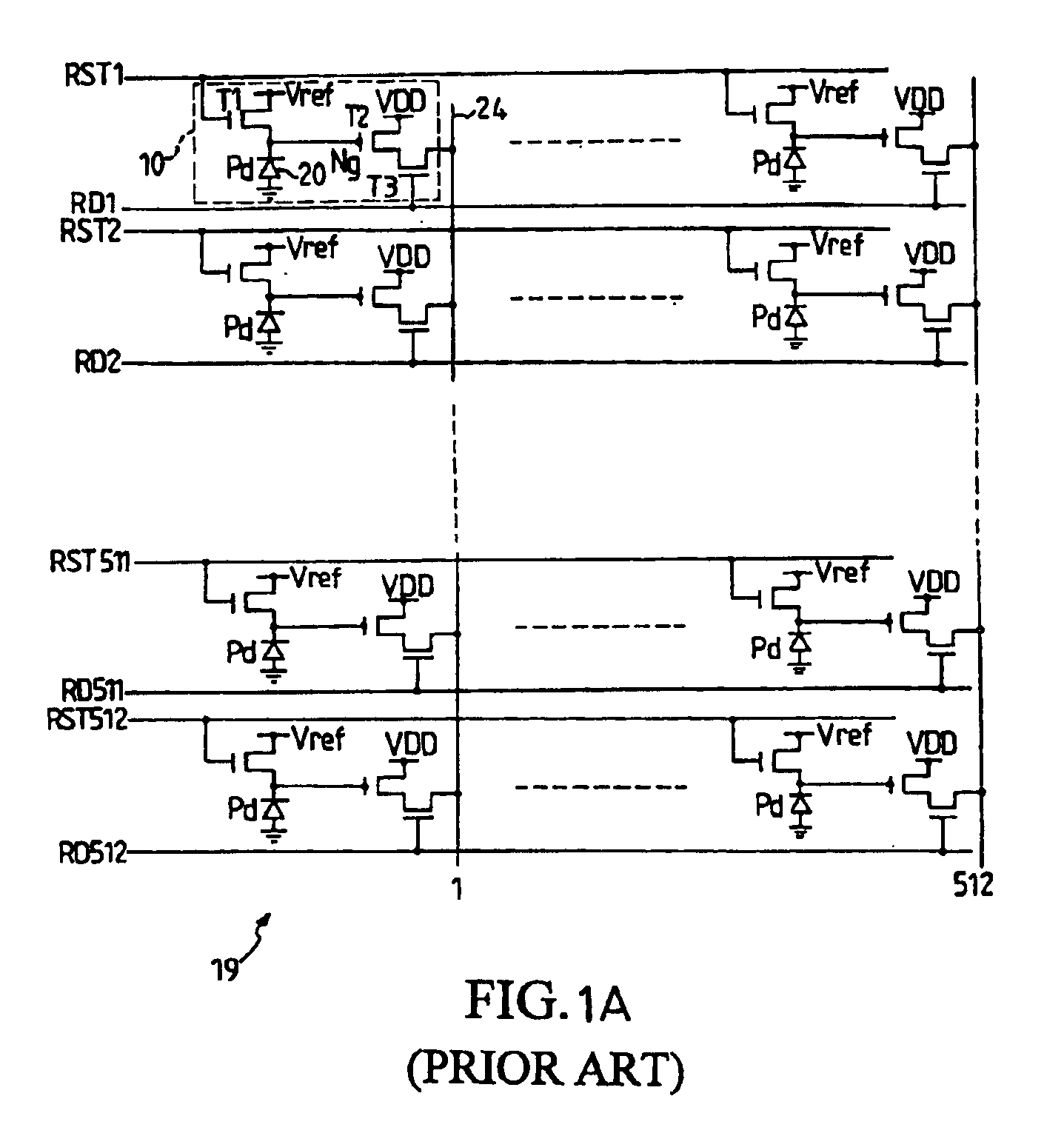
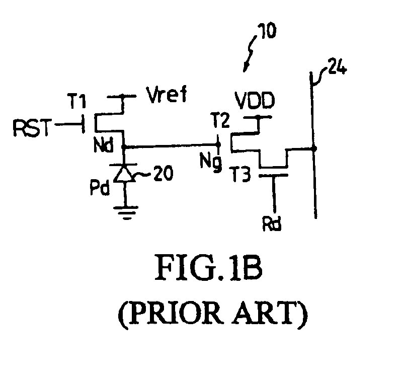
The present application now will be described more fully (hereinafter parenthesized with reference to the accompanying drawings), in which embodiments of the invention are shown. Although one of the embodiments illustrated relates to a CMOS image sensor application, those skilled in the art will appreciate that this invention may be embodied in many different forms set forth herein. These embodiments are provided so that this disclosure will be thorough and complete, and will fully convey the scope of the invention to those skilled in the art.

Reference now will be made in detail to the preferred embodiments of the present invention as illustrated in the accompanying drawings in which like reference numerals designate like or corresponding elements throughout the drawings.

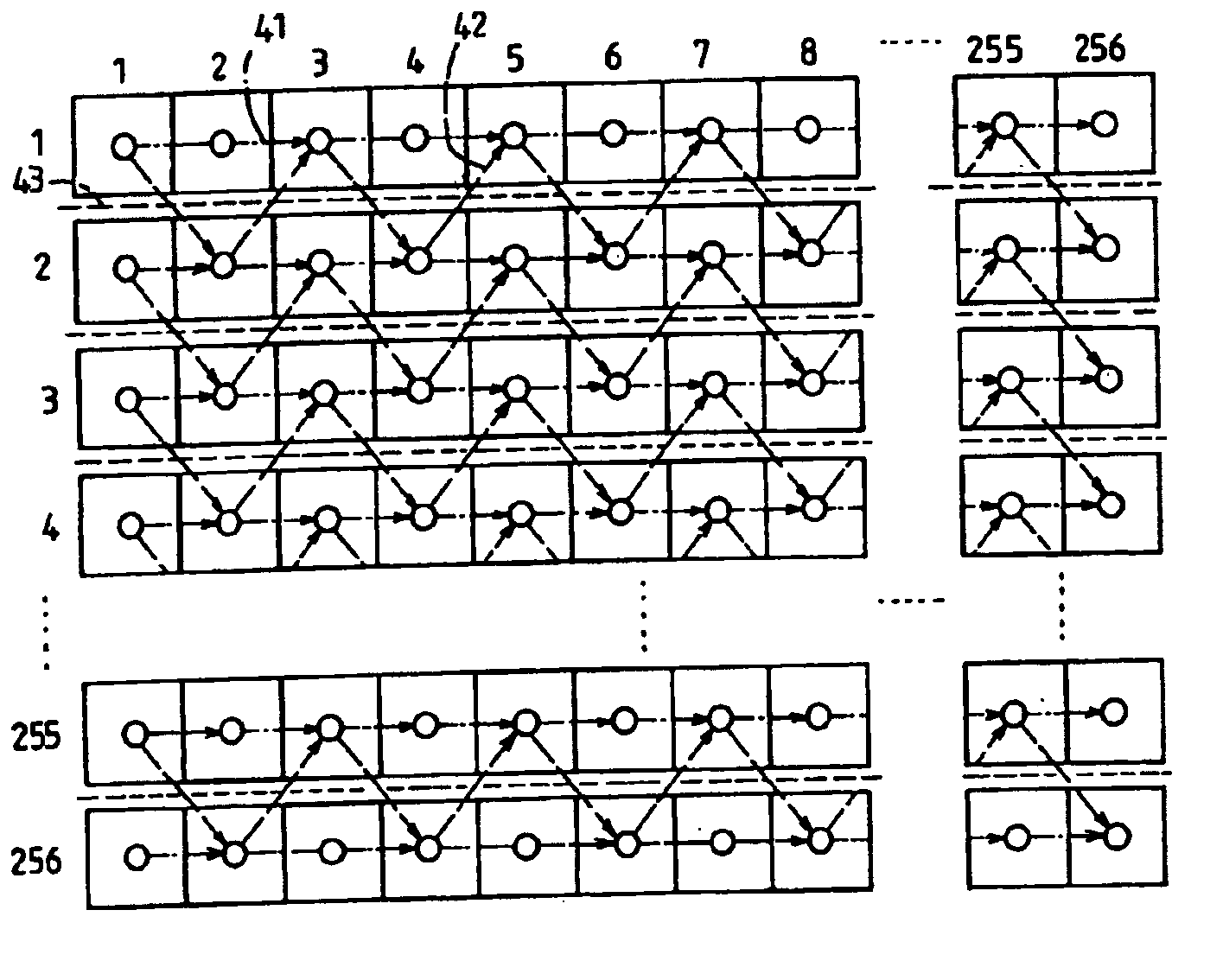
FIG. 2A illustrates a CMOS image sensor array of 256 by 256 active pixels according to one preferred embodiment. Though the numbers of these pixels have been reduced for purposes of illustration, it should be unders...


PUM


Abstract

A structure of an image sensor for sensing the light of an image impinging thereupon and for translating the image into a standard television format is disclosed. The structure comprises a plurality of first and second light detecting elements (22, 23) arranged in rows and columns and half as many rows and columns as scan lines of a television format for generating respective analog signals in proportion to the intensity of the light impinging respectively on each of the first and second light detecting elements (22, 23), wherein the first and second light detecting elements in each row are alternately disposed and activated by first read lines RDOn (n=1 . . . 256) to generate odd field signals, and wherein the first and second light detecting elements (22, 23) of two adjacent rows disposed in a zigzag or serrated manner are activated by second read lines RDEn (n=1 . . . 256) to generate even field signals.

Description

FIELD OF INVENTIONThe present invention relates to a CMOS type image sensor and, in particular, to a special pixel arrangement to enhance the sensitivity and picture quality of CMOS type image sensors.BACKGROUND OF INVENTIONAn image sensor is used to transform an optical image focused on the sensor into electrical signals. The image sensor typically contains an array of light detecting-elements, wherein each element produces an analog signal in response to the light intensity of an image impinging on the element when the image is focused on the array. These signals from the sensor array may then be used to display a corresponding image on a monitor.One very well known type of an image sensor is the charge-coupled device (CCD). Integrated circuit chips containing CCD image sensors are expensive because of the specific A manufacture process required. The CCD also requires relatively large power dissipation, because of the required clock signals and the high voltage that is usually nee...

Claims


Application Information

Patent Timeline
IPC IPC(8): H04N3/15H04N5/335H01L27/146
CPCH04N3/155H04N25/441H04N25/766H01L27/146
Inventor LEE, SYWE N.WAYNE, DAVID
Owner ALCOR MICRO CORP
Why Eureka
Try Eureka