Packaged device adapter assembly with alignment structure and methods regarding same

Inactive Publication Date: 2005-04-12
IRONWOOD ELECTRONICS
View PDF88 Cites 29 Cited by
  • Summary
  • Abstract
  • Description
  • Claims
  • Application Information

AI Technical Summary

Benefits of technology

The present invention provides packaged device adapter assemblies useable for high density integrated circuit packages, e.g

Problems solved by technology

For example, such device packages may be relatively expensive.
Further, for example, once attached, the solder spheres are not accessible for testing.
In addition, it is often difficult to rework the circuit board with the packages soldered thereon.
However, the high density of terminals for certain packages, e.g., micro lead frame packages, lead to various interconnect pr

Method used


Image

  • Packaged device adapter assembly with alignment structure and methods regarding same
  • Packaged device adapter assembly with alignment structure and methods regarding same
  • Packaged device adapter assembly with alignment structure and methods regarding same

Examples


Embodiment Construction

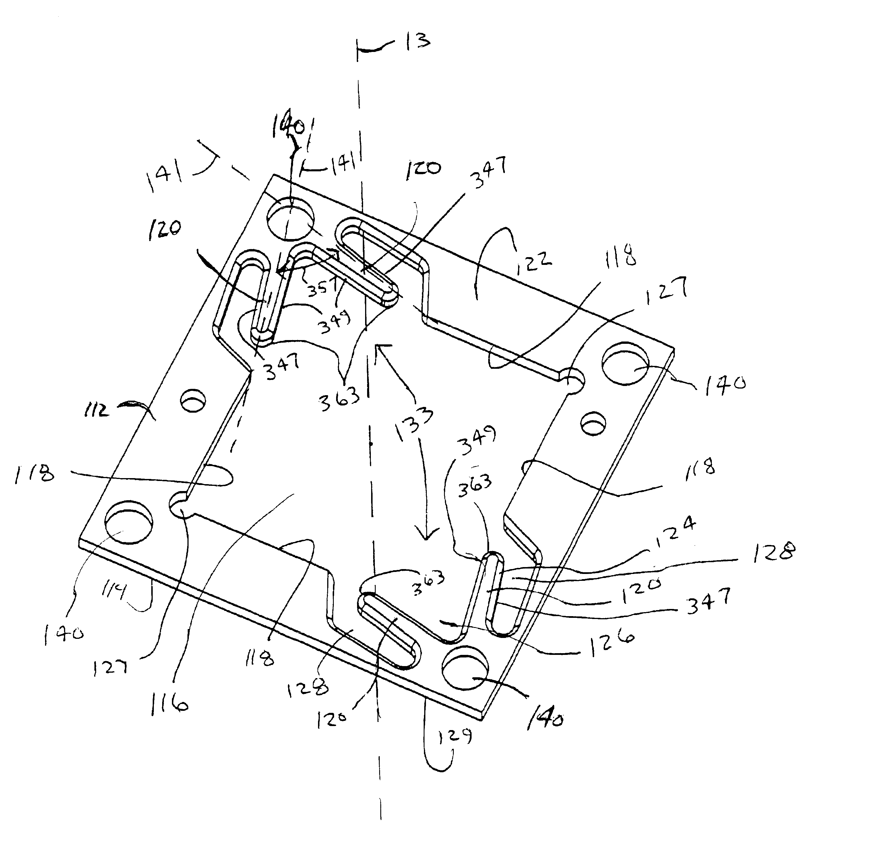
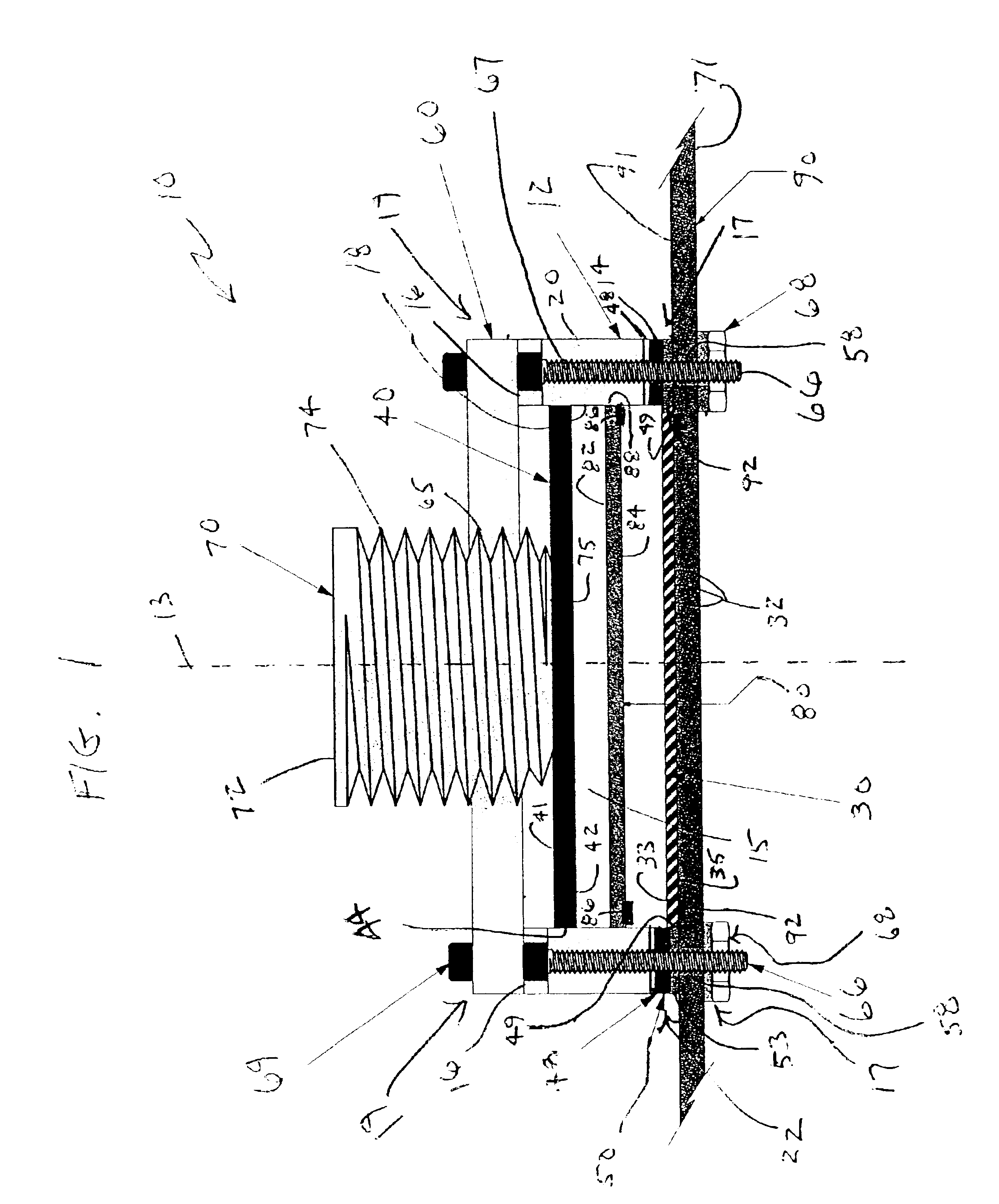
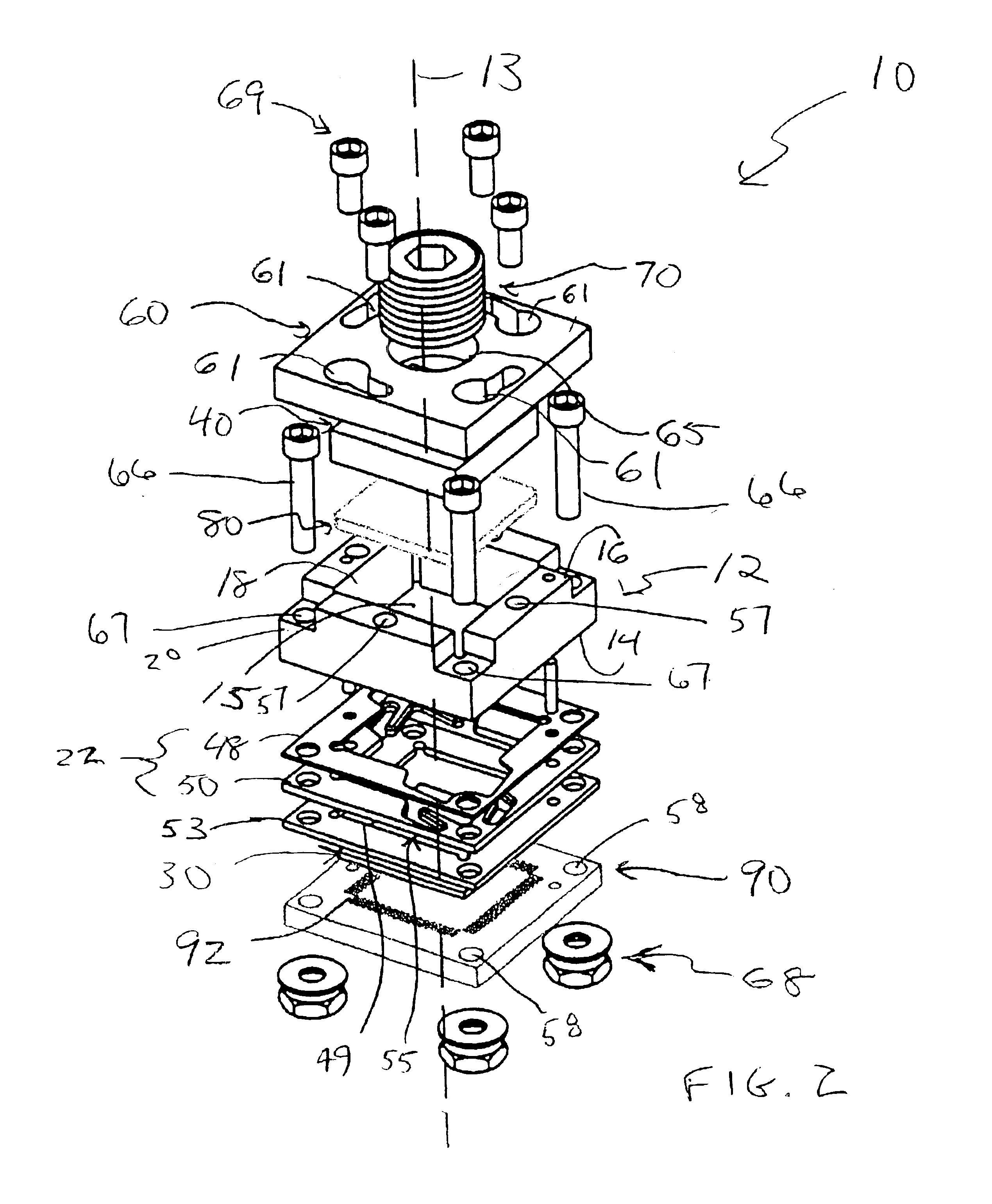
Generally, packaged device adapter assemblies for use with packaged devices, e.g., high density devices, along with methods using such assemblies, shall be described herein. An illustrative packaged device adapter assembly 10 according to the present invention shall be described with reference to illustrative FIGS. 1-2. Various other illustrative embodiments of packaged device adapter assemblies according to the present invention, including features which may be included in combination with features or structure of the other assemblies as described herein, shall be described with reference to FIGS. 3-7.

One skilled in the art will recognize from the description herein, that the various illustrative embodiments described include some features or elements included in other illustrative embodiments and / or exclude other features. However, a packaged device adapter assembly according to the present invention may include any combination of elements selected from one or more of the various ...


PUM


Abstract

A packaged device adapter assembly for use with high density integrated circuit packages, e.g., micro lead frame packages, micro lead chip carriers, quad flat no lead packages, and micro ball grid array packages, etc., includes an alignment structure for aligning a packaged device therein.

Description

BACKGROUND OF THE INVENTIONThe present invention relates to electrical adapters and methods using such adapters. More particularly, the present invention pertains to adapters for packaged integrated circuit devices, e.g., micro lead frame packages, micro lead chip carriers, quad flat no lead packages, and micro ball grid array packages, etc., and methods for using such adapters.Certain types of integrated circuit packages are becoming increasingly popular due to their occupancy area efficiency. In other words, they occupy less area on a target board on which they are mounted while providing a high density of contact terminals. For example, one such high density package type is a micro lead frame package. Generally, such packages contain an integrated circuit having its die bond pads electrically connected to respective conductive contact lead elements (e.g., lands) that are distributed on a surface of the package (e.g., the bottom surface of the package, for example, in an array).A ...

Claims


Application Information

Patent Timeline
IPC IPC(8): H01L23/40H01L23/34
CPCH01L23/4006H01L2224/73253H01L2224/16
Inventor PALANIAPPA, ILAVARASANFEDDE, MICKIELCRAMER, JASON ALLEN
Owner IRONWOOD ELECTRONICS
Why Eureka
Try Eureka