Quad-flat no-leads package structure and method of manufacturing the same

a no-leads, package technology, applied in the direction of semiconductor devices, electrical devices, semiconductor/solid-state device details, etc., can solve the problems of imposing negative effects on production yield and cost, reducing production efficiency, etc., to improve production yield, reduce production costs, and simplify the packaging manufacturing process

Inactive Publication Date: 2015-10-01
LINGSEN PRECISION INDS
View PDF4 Cites 4 Cited by
  • Summary
  • Abstract
  • Description
  • Claims
  • Application Information

AI Technical Summary

Benefits of technology

[0007]It is an objective of the present invention to provide a quad-flat no-leads package (QFN) structure and a method of manufacturing the same based on application of wafer-level chip-scale package (WLCSP) and extension of tape quad-flat no-leads package (tape QFN) to simplify the package manufacturing process, cut production costs, and enhance production yield.
[0031]Accordingly, the quad-flat no-leads package (QFN) structure of the present invention is based on application of WLCSP and extension of tape QFN to simplify the package manufacturing process, cut production costs, and enhance production yield.

Problems solved by technology

However, during the re-distribution step performed with the RDL, the RDL is formed on multiple metal pads within a region, and thus the buildup makes the package larger and renders the manufacturing process more difficult, thereby imposing a negative effect on the production yield and costs.
In conclusion, conventional quad-flat no-leads package (QFN) structures and methods of manufacturing the same have drawbacks and thus there is still room for improvement of the prior art.

Method used


Image

  • Quad-flat no-leads package structure and method of manufacturing the same
  • Quad-flat no-leads package structure and method of manufacturing the same
  • Quad-flat no-leads package structure and method of manufacturing the same

Examples


Embodiment Construction

[0037]Objectives, features, and advantages of the present invention are hereunder illustrated with a first preferred embodiment.

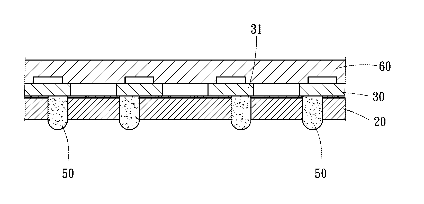
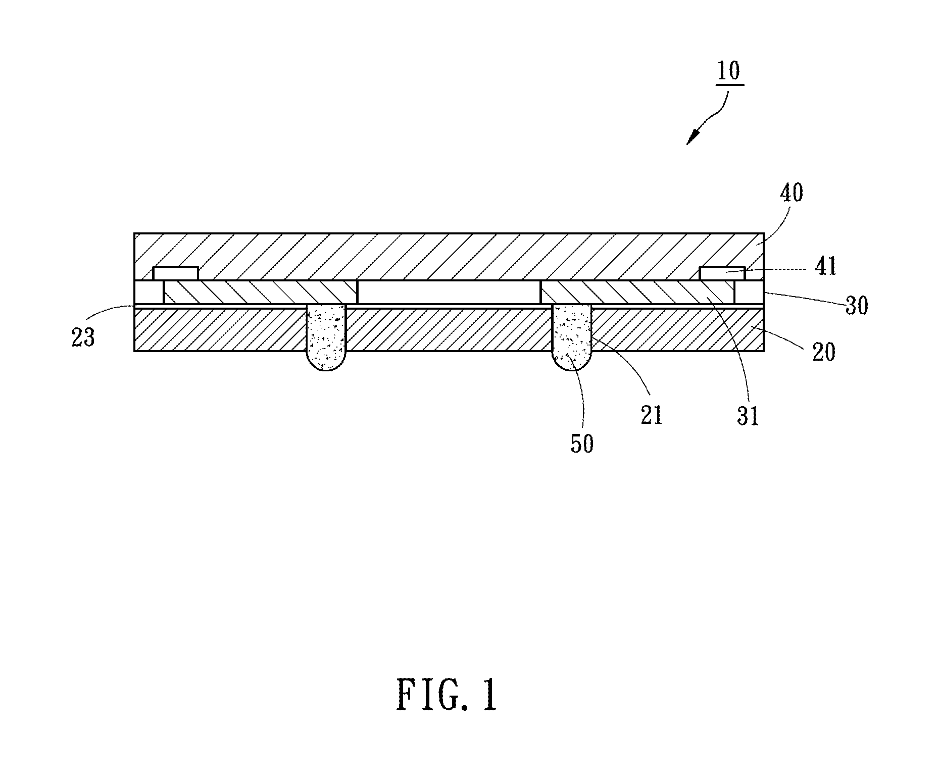
[0038]Referring to FIG. 1, in the first preferred embodiment of the present invention, a quad-flat no-leads package (QFN) structure 10 comprises a thin-film layer 20, a plurality of conduction wirings 31, a die 40, and a plurality of metal bumps 50.

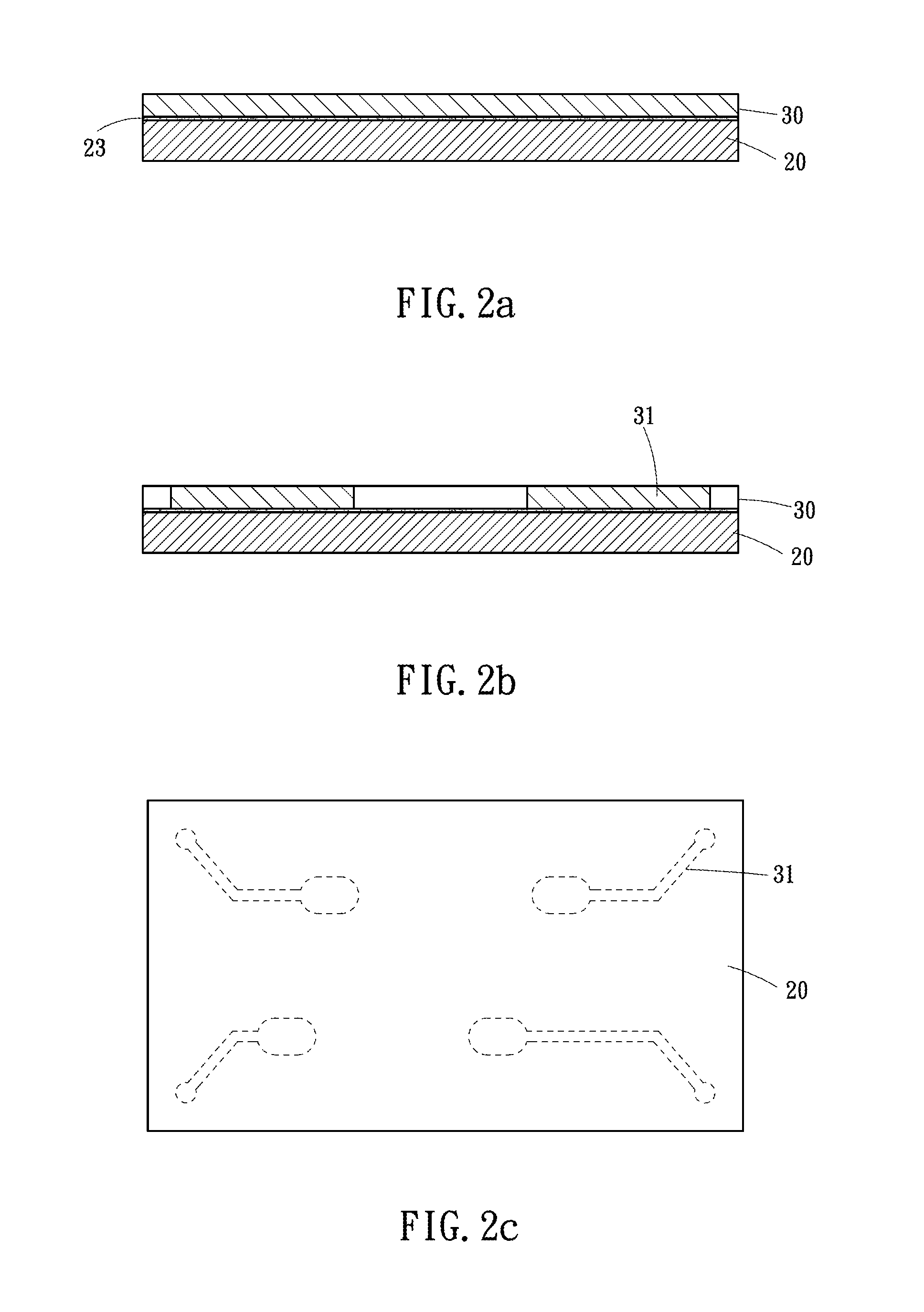
[0039]The thin-film layer 20 has a plurality of through-holes 21. A surface of the thin-film layer 20 faces the conduction wirings 31 and has an adhesive glue 23.

[0040]The conduction wirings 31 lie on the surface of the thin-film layer 20. The terminal ends of the conduction wirings 31 are exposed from the through-holes 21, respectively.

[0041]The die 40 has a plurality of contact pads 41. The contact pads 41 are electrically connected to the conduction wirings 31, respectively.

[0042]The metal bumps 50 are disposed at the through-holes 21, respectively. The metal bumps 50 each have one end connected to a correspon...


PUM


Abstract

A method of manufacturing a quad-flat no-leads package (QFN) structure includes: forming a conducting layer on a surface of a thin-film layer; forming a plurality of conduction wirings from the conducting layer by a means of circuit layout; electrically connecting contact pads of a die to front ends of the conduction wirings, respectively; forming a plurality of through-holes in the thin-film layer by a means of drilling, such that terminal ends of the conduction wirings are exposed from the through-holes, respectively; and forming a plurality of metal bumps at the through-holes, respectively, such that signals from the die are sent to a bottom surface of the thin-film layer through the conduction wirings. Hence, the QFN structure and the method of manufacturing the same based on application of wafer-level chip-scale package (WLCSP) and extension of tape QFN to simplify the package manufacturing process, cut production costs, and enhance production yield.

Description

BACKGROUND OF THE INVENTION[0001]1. Technical Field[0002]The present invention relates to package structures and methods of manufacturing the same, and more particularly, to a quad-flat no-leads package structure and a method of manufacturing the same.[0003]2. Description of Related Art[0004]Ever-changing technologies, together with the high-tech electronic sector's frequent release of multifunction personalized electronic products, bring about the rapid advancements of semiconductor packaging in terms of miniaturization, such as a quad-flat no-leads package (QFN) and a wafer-level chip-scale package (WLCSP), to therefore downsize electronic components, cut production costs, and enhance the electrical properties of the electronic components.[0005]To mount a die on the upper surface of a substrate directly, the sector presently processes QFN products by a re-distribution layer (RDL) technique which entails providing a substrate in the form of a copperfoil layer, performing a layout a...

Claims


Application Information

Patent Timeline
Patent Type & Authority Applications(United States)
IPC IPC(8): H01L23/00H01L23/528H01L21/768H01L21/78H01L21/304
CPCH01L24/14H01L24/11H01L21/78H01L21/304H01L2924/401H01L24/94H01L21/768H01L23/528H01L2224/13025H01L21/76802H01L2924/12042H01L23/3114H01L23/4985H01L21/561H01L2224/02319H01L2224/0233H01L2224/0236H01L24/02H01L24/13H01L24/92H01L2224/02377H01L2224/11334H01L2224/13022H01L2224/13024H01L2224/92H01L2224/94H01L2224/02321H01L2924/00H01L2924/00014H01L2224/0231H01L2924/00012
Inventor TU, MING-TELIN, CHING-IHSU, CHIA-JENLIN, SHENG-JEN
Owner LINGSEN PRECISION INDS
Why Eureka
Try Eureka