Apparatus and method for removing contaminants from semiconductor copper electroplating baths

a technology of electroplating bath and apparatus, which is applied in the direction of electrodialysis, diaphragms, refrigeration components, etc., can solve the problems of generating hazardous materials or other kinds of contaminants, increasing the difficulty of void-free interconnect feature filling via conventional metallization techniques, and high cost of implementation and operation

Inactive Publication Date: 2005-04-12
APPLIED MATERIALS INC
View PDF18 Cites 29 Cited by
  • Summary
  • Abstract
  • Description
  • Claims
  • Application Information

AI Technical Summary

Problems solved by technology

However, as interconnect sizes decrease and aspect ratios increase, void-free interconnect feature fill via conventional metallization techniques becomes increasingly difficult.
Although the various organic additives facilitate the plating process and offer a control element over the interconnect formation processes, they ...

Method used


Image

  • Apparatus and method for removing contaminants from semiconductor copper electroplating baths
  • Apparatus and method for removing contaminants from semiconductor copper electroplating baths
  • Apparatus and method for removing contaminants from semiconductor copper electroplating baths

Examples


Embodiment Construction

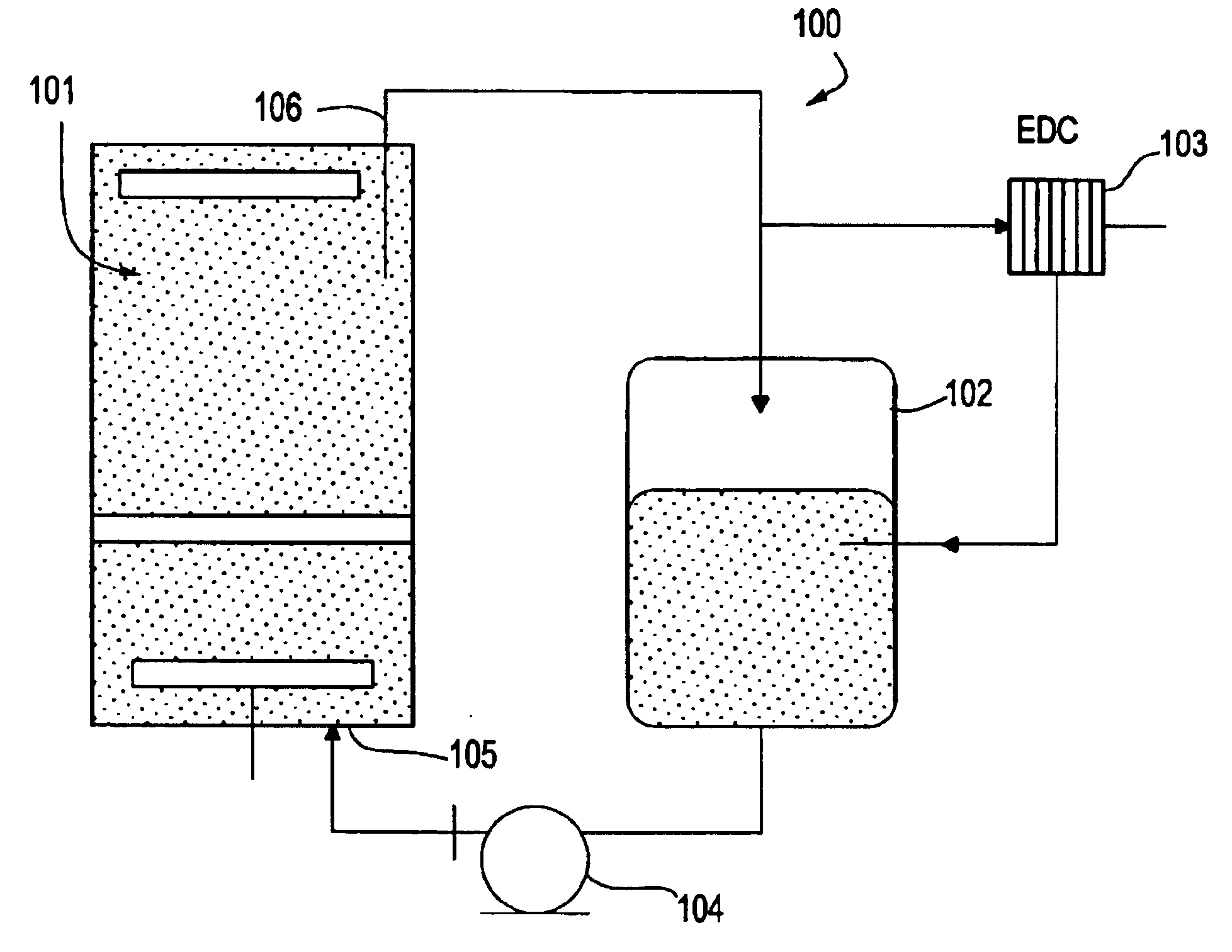
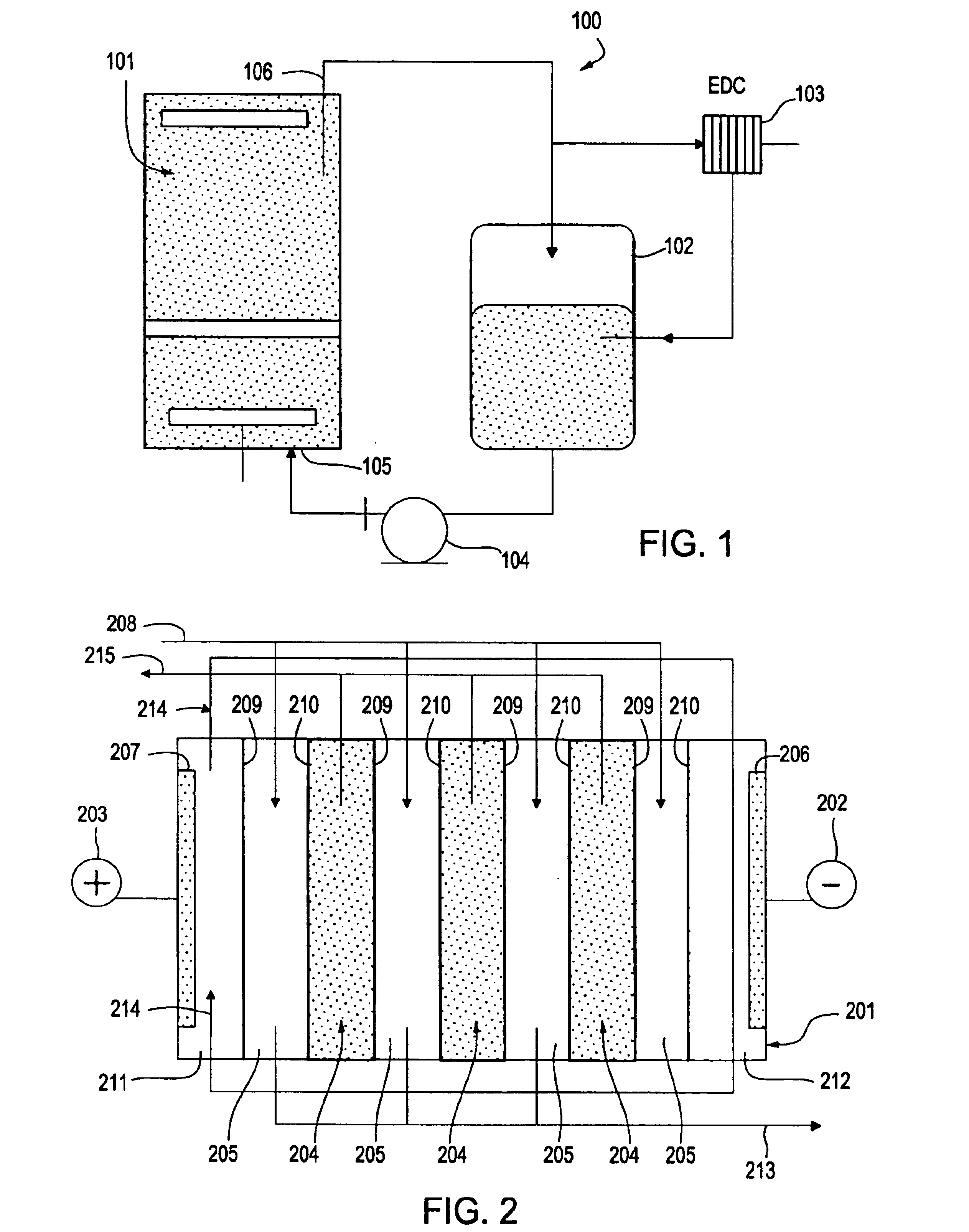
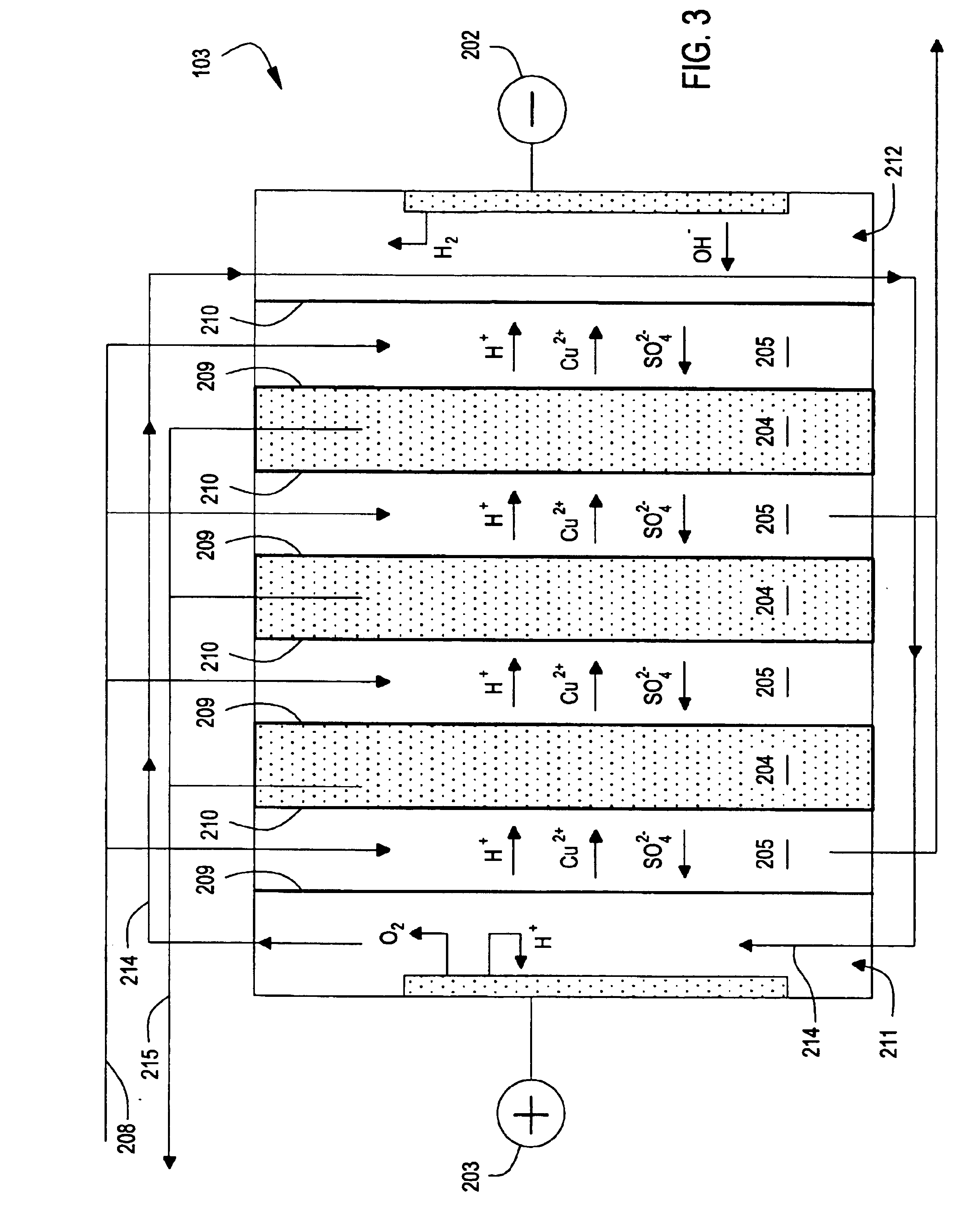
FIG. 1 illustrates an exemplary plating system 100 of the present intention. Plating system 100 generally includes a plating cell 101, which may be electrochemical plating (ECP) cell, an electroless plating cell, or other plating cell configuration known in the semiconductor art. The plating cell 101 generally includes a fluid inlet 105 configured to deliver a plating processing fluid to the plating cell 101, and a fluid outlet or drain 106 configured to retrieve plating processing fluids from plating cell 101. The plating processing fluids are delivered to plating cell 101 via inlet 105, which is in fluid communication with a plating fluid storage unit 102. A fluid pump 104 is generally positioned between the fluid storage unit 102 and the plating cell 101 and is configured to deliver the plating fluid to plating cell 101 upon actuation thereof. The fluid outlet 106 of plating cell 101 is also in fluid communication with the fluid storage unit 102, and therefore, the fluid outlet m...


PUM

PropertyMeasurementUnit
Fractionaaaaaaaaaa
Fractionaaaaaaaaaa
Concentrationaaaaaaaaaa

Abstract

The present invention generally provides an apparatus and method for removing contaminants from a plating solution. The apparatus generally includes a plating cell having an electrolyte inlet and an electrolyte drain, an electrolyte storage unit in fluid communication with the electrolyte inlet, and an electrodialysis chamber in fluid communication with the electrolyte drain, wherein the electrodialysis chamber is generally configured to receive a portion of used electrolyte solution and remove contaminants therefrom. The method generally includes supplying an electrolyte solution to a copper plating cell, plating copper onto a substrate in the plating cell with the electrolyte solution, removing used electrolyte solution from the plating cell, and refreshing a portion of the used electrolyte solution with an electrodialysis cell.

Description

BACKGROUND OF THE INVENTION1. Field of the InventionThe present invention generally relates to removing organic contaminants from semiconductor electrolyte solutions.2. Description of the Related ArtMetallization for sub-quarter micron sized features is a foundational technology for present and future generations of integrated circuit manufacturing processes. More particularly, in devices such as ultra large scale integration-type devices, i.e., devices having integrated circuits with more than a million logic gates, the multilevel interconnects that lie at the heart of these devices are generally formed by filling high aspect ratio interconnect features with a conductive material, such as copper or aluminum. Conventionally, deposition techniques such as chemical vapor deposition (CVD) and physical vapor deposition (PVD) have been used to fill these interconnect features. However, as interconnect sizes decrease and aspect ratios increase, void-free interconnect feature fill via conv...

Claims


Application Information

Patent Timeline
IPC IPC(8): B01D61/42B01D61/44B01D61/52C25D21/18C25D21/00
CPCB01D61/44C25D21/18B01D61/52Y10S204/13
Inventor KOVARSKY, NICOLAY
Owner APPLIED MATERIALS INC
Why Eureka
Try Eureka