
Optical wiring circuit, optical wiring circuits layered body and opto-electric wiring apparatus

a wiring circuit and optical wiring technology, applied in the field of optical interconnection technique, can solve the problems of limiting the processing speed of a system using an electric bus circuit, electromagnetic noise, and more and more difficult for the electric bus circuit to cope with high-speed bus processing, so as to simplify the structure of the opto-electric wiring apparatus and reduce the delay amount. , the effect of easy connection

Inactive Publication Date: 2005-04-12
FUJIFILM BUSINESS INNOVATION CORP
View PDF10 Cites 7 Cited by
  • Summary
  • Abstract
  • Description
  • Claims
  • Application Information

AI Technical Summary

Benefits of technology

The invention provides an opto-electric wiring apparatus that can connect optical wiring circuits and electric wiring circuits easily. The apparatus includes a layered body with multiple optical wiring circuits and an opto-electric conversion element. The optical wiring circuits are connected to the electric wiring circuit through an opto-electric conversion element, which simplifies the structure and reduces delay. The apparatus can have more connection points by combining the optical wiring circuits and the electric wiring circuit.

Problems solved by technology

However, in the case of the electric bus circuit, a signal delay caused by inter-connection-wiring capacity and connection wiring resistance limits the processing speed of a system using the electric bus circuit.
When trying to make more dense a parallel-bus connection wiring, there arises a problem that an electromagnetic noise occurs; that is, it has been more and more difficult for the electric bus circuit to cope with the high-speed bus processing.
However, in the disclosed technique, since light / electricity conversion is necessary for every communication between the mutually adjoining circuit boards, the cost is expensive and the delay amount is large.
Also, because the light is transmitted through a free space, the optical / electric element is difficult to position and is also weak against crosstalk and dust.
However, in the disclosed structure, no attention is paid to arrangement and structure of the other end of the optical wave guide; that is, the other end of the optical wave guide is extended from the side surface of the optical circuit board and thus, to connect the optical circuit board with another optical circuit board or an electric wiring circuit, the optical wave guide must be bent in a complicated manner, which makes it difficult to position the other end of the optical wave guide.

Method used


Image

  • Optical wiring circuit, optical wiring circuits layered body and opto-electric wiring apparatus
  • Optical wiring circuit, optical wiring circuits layered body and opto-electric wiring apparatus
  • Optical wiring circuit, optical wiring circuits layered body and opto-electric wiring apparatus

Examples


Embodiment Construction

Next, description will be given below of the preferred embodiments according to the invention with reference to the accompanying drawings.

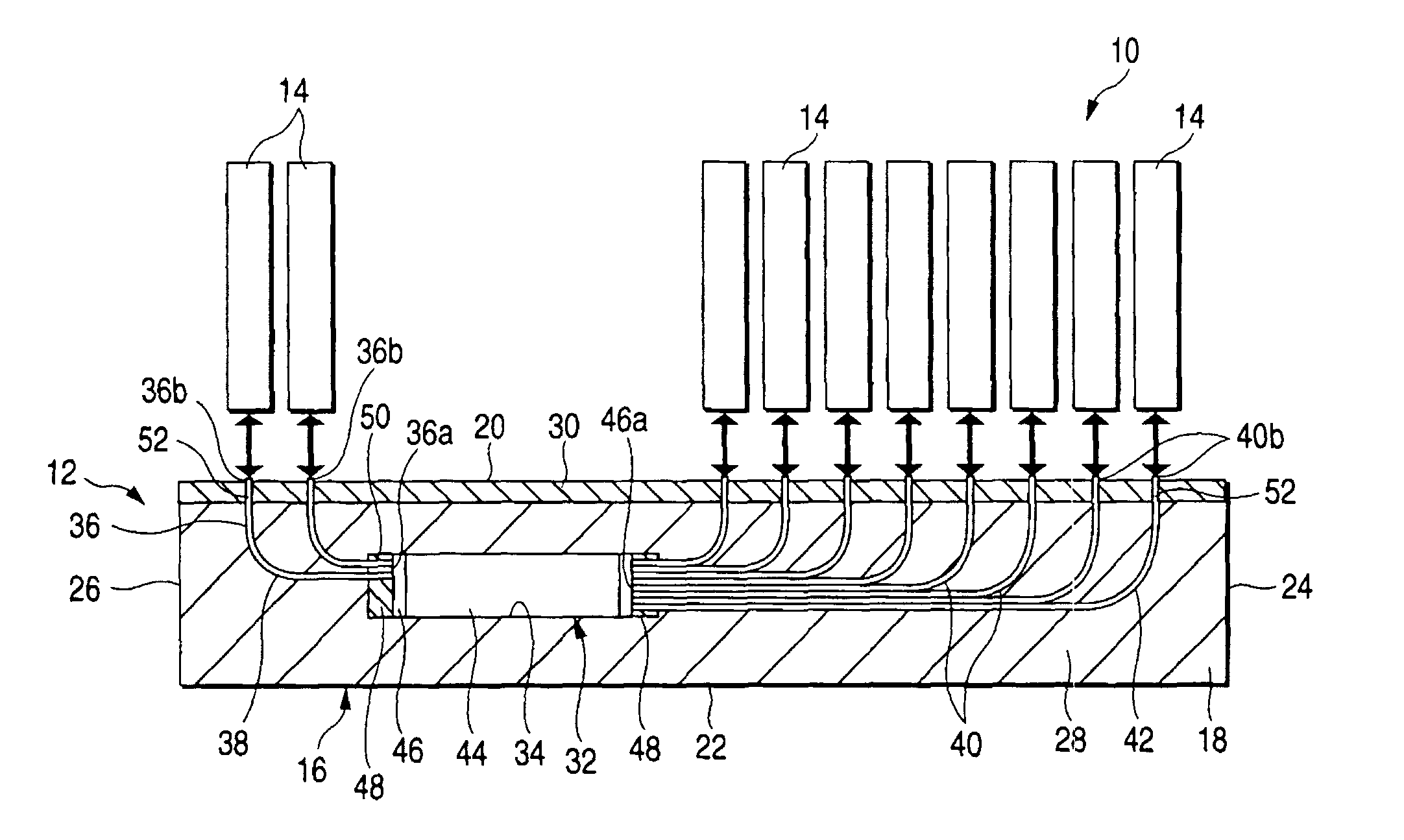
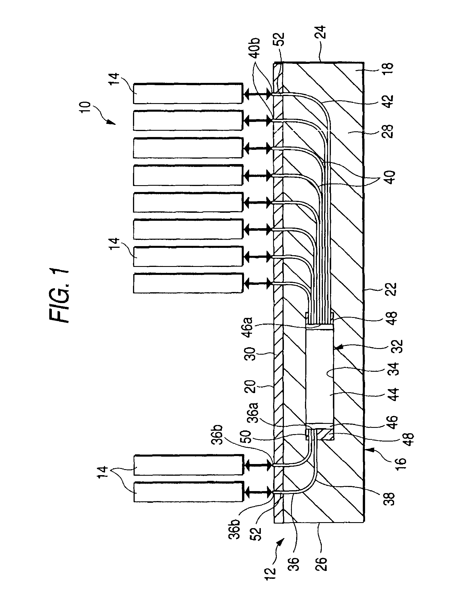
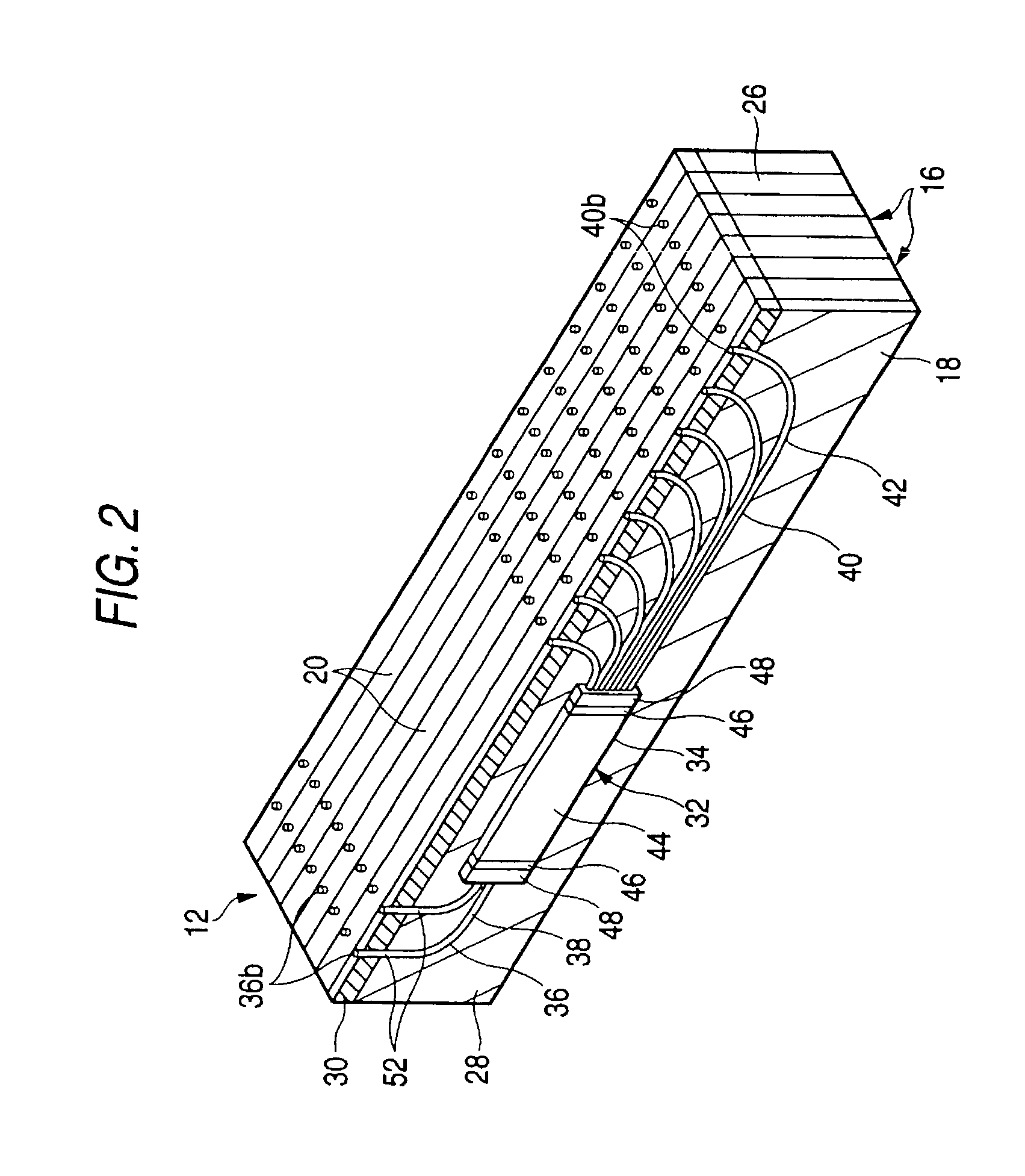
Now, FIGS. 1 and 2 show a first embodiment according to the invention, in which an opto-electric wiring apparatus 10 comprises an optical wiring circuits layered body 12 and a plurality of electric wiring circuits 14. The optical wiring circuits layered body 12 includes a plurality of sheet-shaped optical wiring circuits 16 (in the present embodiment, 8 optical wiring circuits) and is structured such that the optical wiring circuits 16 are superimposed on one another in a sheet side surface direction. The electric wiring circuits 14 respectively include CPUs and memories as well as are optically connected to the optical wiring circuits 16.

Each of the optical wiring circuits 16 includes an optical wiring circuit board 18 formed in a sheet shape, while the optical wiring circuit board 18 includes two side surfaces as well as an upper surface 20, a l...


PUM


Abstract

A first optical wave guide 36 and a second optical wave guide 40 are connected to both sides of a planer optical waveguide 32, respectively. The other ends 36b, 40b of the first and second optical wave guides 36, 40 are extended over an upper surface 20 of an optical wiring circuit board 18. An electric wiring circuit 14 is connected to the other ends 36b, 40b of the first and second optical wave guides 36, 40, thereby constituting an optical wiring circuit 16. A plurality of optical wiring circuits 16 are superimposed on one another to thereby form an optical wiring circuits layered body 12. The electric wiring circuit 14 can be connected from one surface of the optical wiring circuit board 18, which makes it possible to facilitate the connection thereof.

Description

BACKGROUND OF THE INVENTION1. Field of the InventionThe present invention relates to an optical interconnection technique and, in particular, to the structure of an optical wiring circuit.2. Description of the Related ArtTo connect together a plurality of microprocessors and memories there has been generally used an electric bus circuit. However, in the case of the electric bus circuit, a signal delay caused by inter-connection-wiring capacity and connection wiring resistance limits the processing speed of a system using the electric bus circuit. When trying to make more dense a parallel-bus connection wiring, there arises a problem that an electromagnetic noise occurs; that is, it has been more and more difficult for the electric bus circuit to cope with the high-speed bus processing. In view of this, there has been proposed an optical interconnection technique in which the electric wiring is replaced with an optical wiring to enhance the speed of the bus.For example, in JP-B-Hei. ...

Claims


Application Information

Patent Timeline
Patent Type & Authority Patents(United States)
IPC IPC(8): G02B6/28G02B6/38G02B6/42G02B6/43G02B6/00H01L27/15
CPCG02B6/2808G02B6/2817G02B6/43G02B6/42G02B6/3807
Inventor YAMADA, HIDENORIFUNADA, MASAOKAMIMURA, TAKESHIOKADA, JUNJIKYOZUKA, SHINYASAKAI, KAZUHIROHAMADA, TSUTOMUOZEKI, SHINOBUTAKANASHI, OSAMUMIURA, MASAAKINIITSU, TAKEHIROBABA, TOMOHISADA, MASASHIKOBAYASHI, KENICHI
Owner FUJIFILM BUSINESS INNOVATION CORP
Learn More