

Control method of nonvolatile memory
a control method and nonvolatile technology, applied in the direction of digital storage, instruments, error detection/correction, etc., can solve the problems of short life time in such a system, large obstacle to realizing high-speed processes, and reduce the speed of generating logical-physical address conversion tables, so as to achieve high-speed operation and reduce risk a large degr
- Summary
- Abstract
- Description
- Claims
- Application Information
AI Technical Summary
Benefits of technology
Problems solved by technology
Method used
Image

Examples
embodiment 1
[0041]FIG. 9 is a detailed flowchart of a redundant area data generation process section in FIG. 7 of the present invention.
[0042]FIG. 10 is a schematic flowchart of a logical-physical address conversion table generation process of the present invention at the time of turning a power supply on.
embodiment 2
[0043]FIG. 11 is a schematic flowchart of a writing process of one block of the present invention.
[0044]FIG. 12 is a detailed flowchart of a redundant area data generation process section in FIG. 7 of the embodiment 2 of the present invention.
embodiment 4
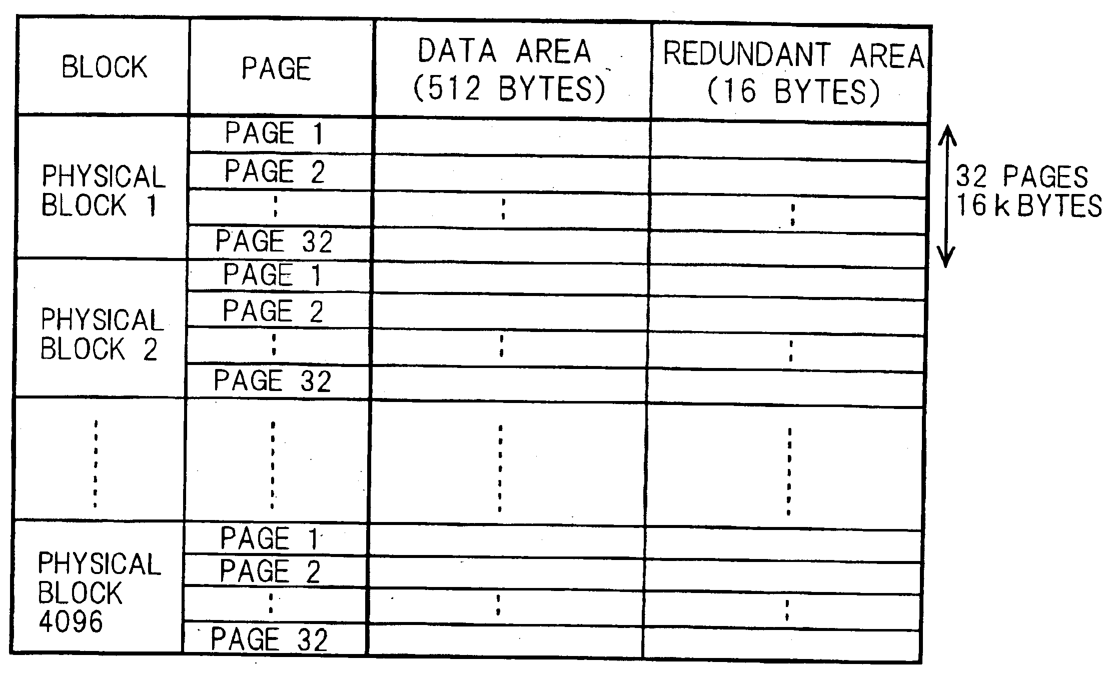
[0045]FIG. 13 is an example of a drawing showing a configuration in a flash memory physical block of the present invention.
[0046]It will be appreciated that all or part of the drawings are purely diagrammatic for illustrative purposes and do not necessarily present faithful depictions of the actual relative sizes and positions of the illustrated elements.
BEST MODE FOR CARRYING OUT THE INVENTION
[0047]Embodiments illustrating the best mode for carrying out the invention will be described below by way of example with reference to the accompanying drawings.
[0048]>
[0049]Using FIGS. 1, 6, 7 and 9, a memory device of an embodiment 1 of the present invention will be explained.
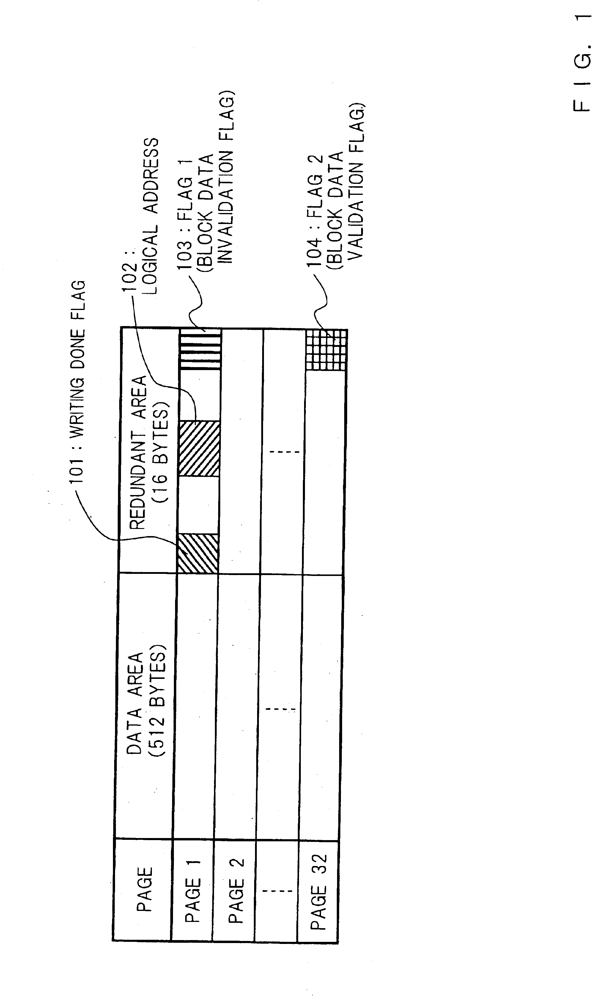
[0050]FIG. 1 is an example of a drawing showing a configuration in a physical block of a flash memory of an embodiment 1 of the present invention. FIG. 1 shows main data written in a redundant area of one physical block. In a redundant area of a top page, three of a writing done flag 101, a logical address 102 and a fl...
PUM
 Abstract
Description
Claims
Application Information