Substrate bias generator in semiconductor memory device

Inactive Publication Date: 2005-04-19
SAMSUNG ELECTRONICS CO LTD
View PDF9 Cites 27 Cited by
  • Summary
  • Abstract
  • Description
  • Claims
  • Application Information

AI Technical Summary

Benefits of technology

[0007]It is therefore object of the present invention to provide a substrate bia

Problems solved by technology

This specially causes the consumption of the operational current to be increased during a stand-by state.
However, since time of the stand-by state is not determined in the operation of the general semiconductor memory device, it is impossible to reduce the current consumption under the stand-by state according to the above method.
Nevertheless, the current consumption generated

Method used


Image

  • Substrate bias generator in semiconductor memory device
  • Substrate bias generator in semiconductor memory device
  • Substrate bias generator in semiconductor memory device

Examples


Embodiment Construction

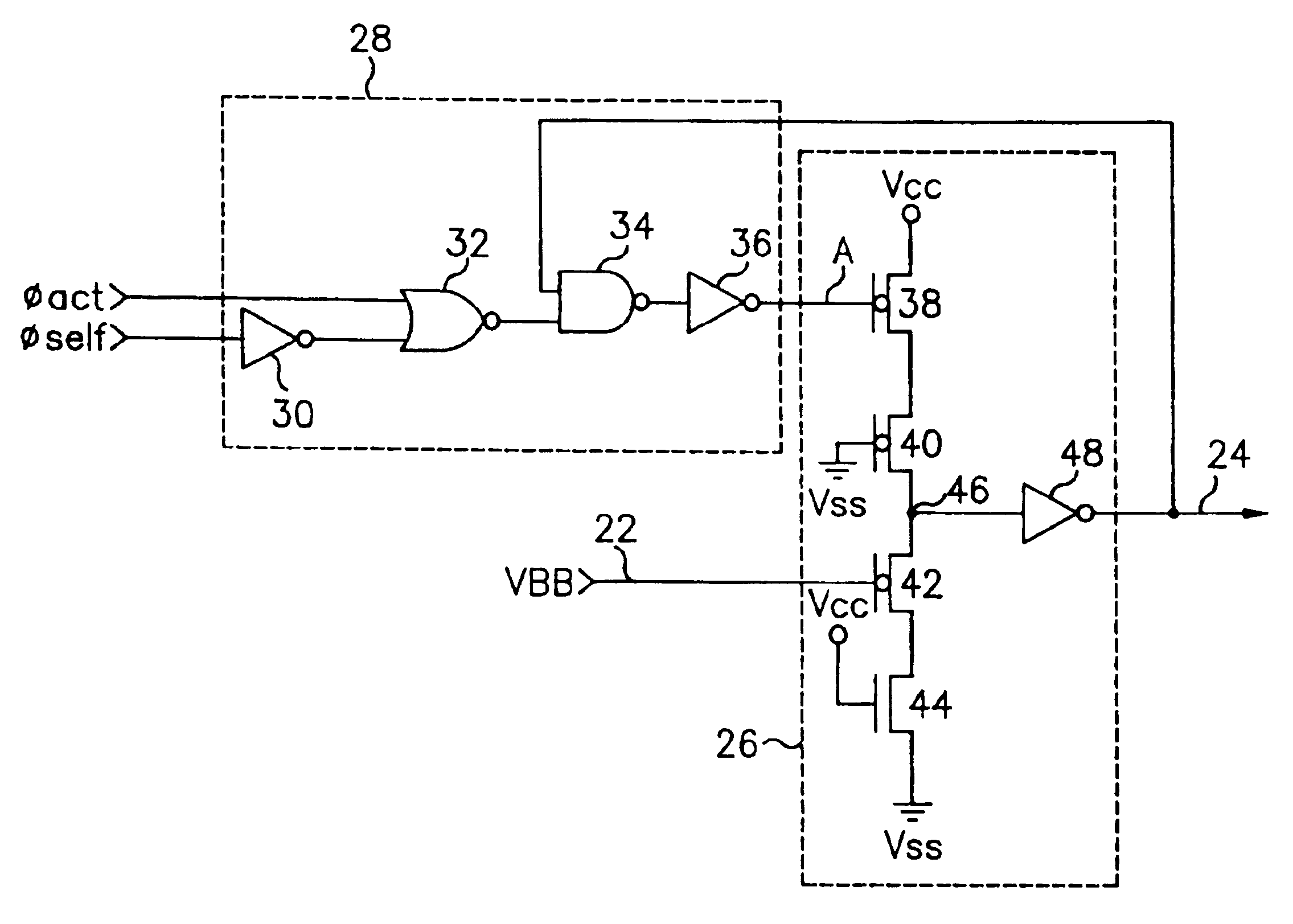
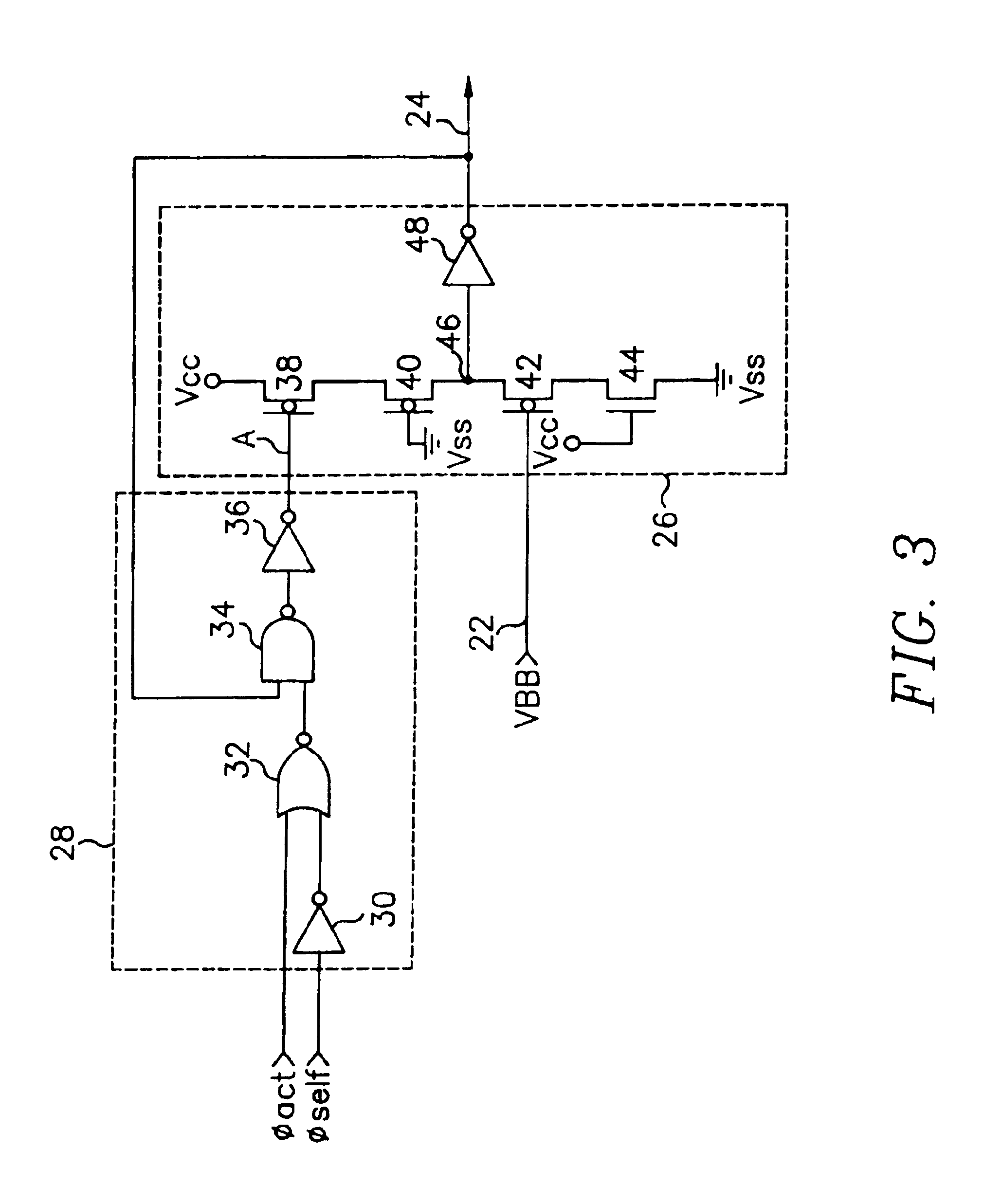
[0021]The point of the description of the preferred embodiment of the present invention is that a substrate bias generator is to prevent the consumption current generated during a stand-by state of a self refresh mode. Therefore, for convenience of the explanation, in the following description, a term “active state” is defined as that of the self refresh mode and another term “stand-by state” as that of the self refresh mode, except a determined case like an “active state of a chip” or a “stand-by state of the chip”. Further, a signal φself of signals mentioned hereinafter indicates an enable signal and another signal φact thereof indicates an active signal of the self refresh mode.

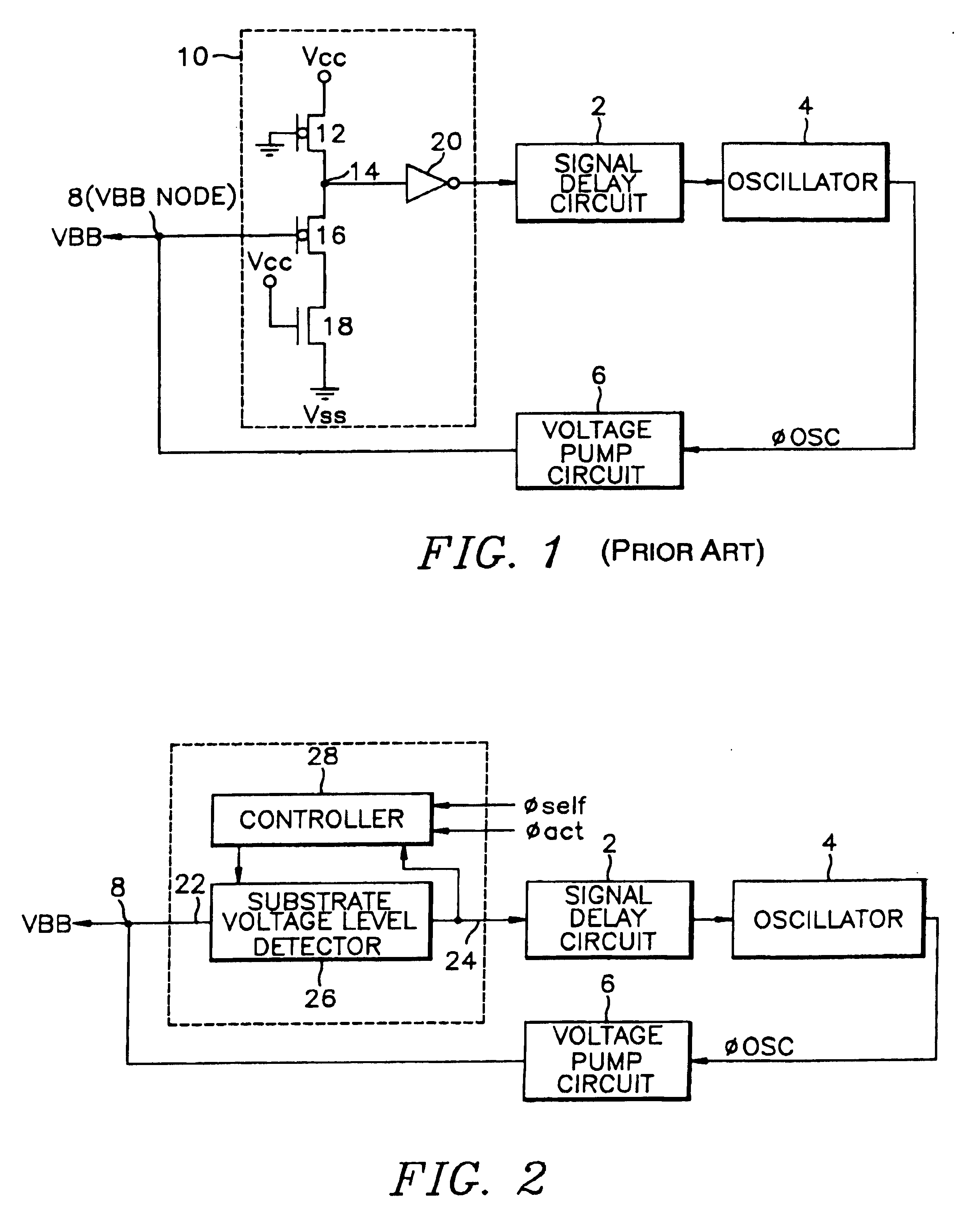
[0022]FIG. 2 is a schematic block view of the substrate bias generator having a substrate voltage level detector according to the present invention. In the construction FIG. 2, a portion indicated by a dotted line block, is a new construction according to the present invention and is the subject matter of...


PUM


Abstract

A substrate bias generator which makes device characteristics stable by supplying a predetermined negative voltage to a substrate and minimally reduces current consumption during a self refresh mode. The substrate bias generator comprises a substrate voltage level detector for inputting a substrate voltage and outputting a signal which drives an oscillator in response to the input level, and a controller for inputting a chip active enable signal, a self refresh mode enable signal and an output signal of the substrate voltage level detector and controlling a switching operation of the substrate voltage level detector in response to the input level.

Description

[0001]This is a continuation of appln. Ser. No. 08 / 691,822; filed Aug. 5, 1996, abandoned upon the filing hereof; which is a continuation of appln. Ser. No. 08 / 596,423; filed Feb. 2, 1996 (abandoned); which is a continuation of appln. Ser. No. B08 / 376,347; filed Jan. 23, 1995 (abandoned).BACKGROUND OF THE INVENTION[0002]The present invention relates to a semiconductor memory device, and more particularly to a substrate bias generator which makes device characteristics stable by supplying a predetermined negative voltage to a substrate and minimally reduces current consumption during a self refresh mode.[0003]In general, a P-type substrate is employed in a dynamic RAM having a memory cell which is composed of one access transistor and one storage capacitor. Further, it is well known that a substrate bias generator must be included in the use of the P-type substrate, the substrate bias generator supplying a negative voltage of a predetermined level to the substrate. In the meantime, t...

Claims


Application Information

Patent Timeline
IPC IPC(8): G05F1/10G05F3/20
CPCG05F3/205
Inventor LEE, HEE-CHUN
Owner SAMSUNG ELECTRONICS CO LTD
Why Eureka
Try Eureka