Field emission displaying device and driving method thereof

a technology of emission display and display device, which is applied in the direction of static indicating device, instruments, etc., can solve the problems of high power consumption, difficult to precisely match the same emitter with each other, and consume a lot of time in the process of fabricating the emitter, etc., to achieve uniform cell, picture quality and effect of uniformity

Inactive Publication Date: 2005-04-19
LG ELECTRONICS INC
View PDF8 Cites 3 Cited by
  • Summary
  • Abstract
  • Description
  • Claims
  • Application Information

AI Technical Summary

Benefits of technology

[0037]Therefore, an object of the present invention is to provide a field emission displaying apparatus and method in which uniformity of cell is obtained by supplying a reset pulse to every scan line after supplying a scan pulse to one scan line and since every cell is driven in a uniform state, a picture quality and an efficiency of a field emission display device are improved.

Problems solved by technology

Thus, emitters are to be fabricated to be uniform, but with the current fabricating process, it is not easy to fabricate emitters exactly the same with each other and much time is consumed for the process for fabricating the emitters.
In addition, since electrons are emitted from the acute emitter, scores of bolt and hundreds of bolt voltage should be applied to a cathode electrode and a gate electrode, causing a problem of much power consumption.
In other words, in the conventional flat type FED, when the scan pulse is applied to one scan line, since the data pulse is applied to every scan line, the cells are not uniform.
In addition, the driving speed is degraded due to the value of the capacitance charged in the cells that are not operated, so that the driving efficiency is degraded.
In addition, a displacement current having a great peak value increases a reactive power that is not contributed to emitting, causing a problem of a power loss.

Method used


Image

  • Field emission displaying device and driving method thereof
  • Field emission displaying device and driving method thereof
  • Field emission displaying device and driving method thereof

Examples


first embodiment

[0062]FIG. 4 is a drawing illustrating waveforms according to a driving method of a field emission display device in accordance with the present invention.

[0063]As shown in FIG. 4, a scan pulse (SP) of negative polarity is sequentially supplied to scan lines (S1, S2, . . . , Sm) of an FED, and a data pulse (DP) of positive polarity synchronized with the scan pulse (SP) is supplied to data lines (D1, D2, . . . , Dm). Whether the data pulse (DP) is to be applied or not to the data lines (D1, D2, . . . , Dm) is determined on a picture to be displayed.

[0064]After the data pulse is supplied to the data lines (D1, D2, . . . , Dm), a reset pulse (RP) is supplied to every scan line (S1, S2, . . . , Sm). The reset pulse (RP) is supplied between the scan pulse (SP) supplied to one scan line (Si) and a scan pulse (SP) supplied to the next scan line (Si+1).

[0065]For example, when −5V scan pulse (SP) is applied to a first scan line (S1) and 5V data pulse (DP) is applied to the data lines (D1, D2...

second embodiment

[0069]FIG. 5 is a drawing illustrating waveforms according to a driving method of a field emission display device in accordance with the present invention.

[0070]As shown in FIG. 5, a scan pulse (SP) of negative polarity is sequentially supplied to the scan lines (S1, S2, . . . , Sm) of the FED and a data pulse (DP) of positive polarity synchronized with the scan pulse (SP) is supplied to the data lines (D1, D2, . . . , Dm).

[0071]After the scan pulse (SP) is sequentially supplied to every scan line (S1, S2, . . . , Sm), at least more than 2 reset pulses (RP) are supplied to the scan lines. Then, the residual electric charges of the cells are all removed, so that a uniformity of the cell can be improved.

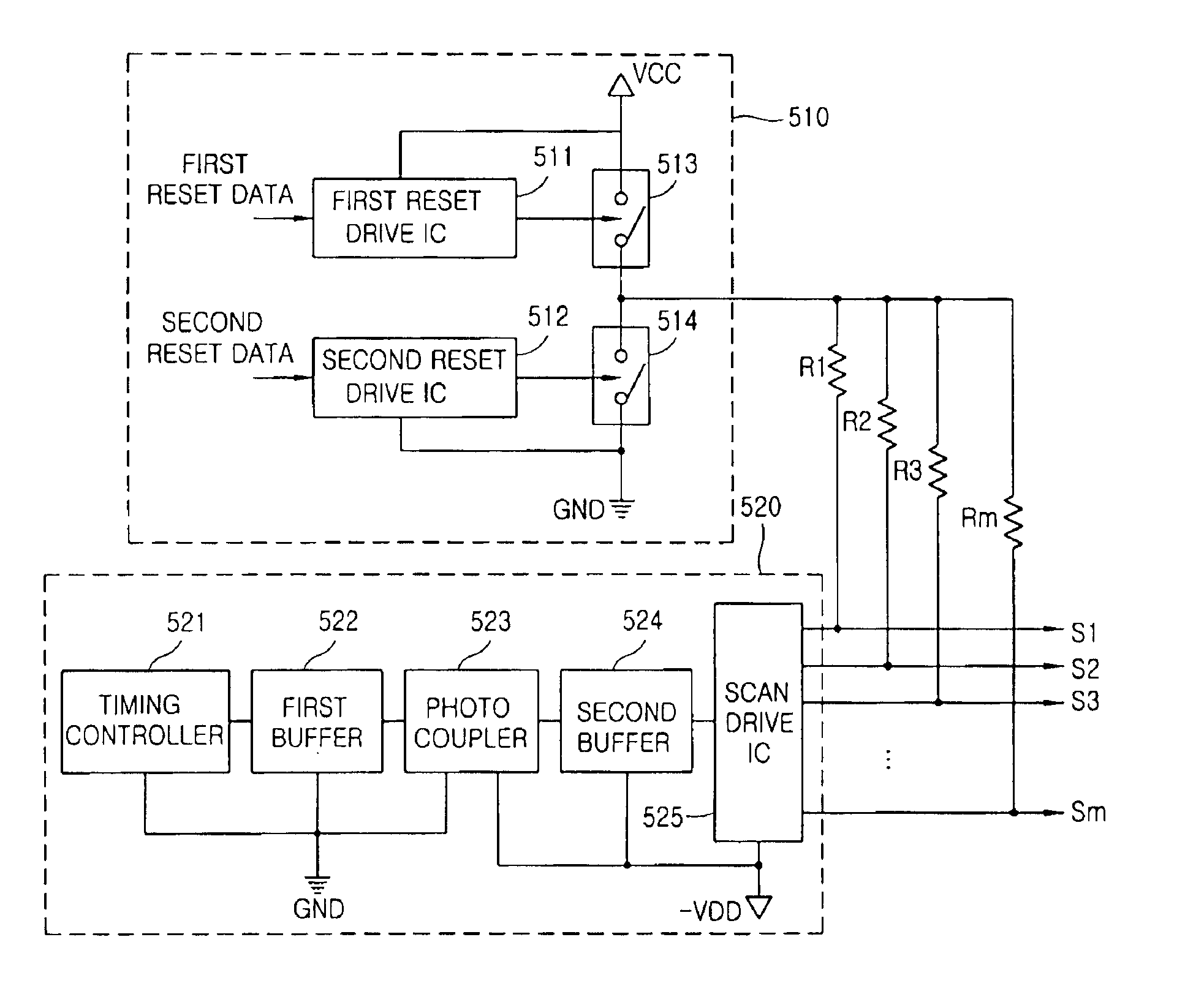
[0072]FIG. 6 is a schematic block diagram showing a driving circuit for generating driving waveforms at each scan line in accordance with the present invention.

[0073]As shown in FIG. 6, the driving circuit includes a reset driving unit (510) for supplying the reset pulse (RP) to the sc...

third embodiment

[0108]FIG. 9 is a drawing illustrating waveforms according to a driving method of a field emission display device in accordance with the present invention.

[0109]As shown in FIG. 9, scan pulse (SP) of negative polarity is sequentially supplied to the scan liens (S1, S2, . . . , Sm) of the FET and a data pulse (DP) of positive polarity synchronized with the scan pulse (SP) of negative polarity is supplied to the data line (D).

[0110]Electrons are emitted from the cell to which the scan pulse (SP) and the data pulse (DP) have been supplied, due to the voltage difference between the scan pulse (SP) and the data pulse (DP).

[0111]The driving waveforms will now be described in detail with reference to the accompanying drawings.

[0112]First, when the scan pulse (SP) of negative polarity is applied to the first scan line (S1) and the data pulse (DP) of positive polarity is supplied to the data line (D), a voltage difference between the scan pulse (SP) and the data pulse (DP) occurs at the firs...


PUM


Abstract

A field emission display device includes: a reset driving unit for supplying a reset pulse to a scan line and a scan driving unit for supplying a scan pulse to the scan line. The reset driving unit includes a first reset drive IC for receiving a first reset data from a reset data supplying unit, a second reset drive IC for receiving a second reset data from the reset data supplying unit and a first switch connected to the first reset drive IC and turned on/off by the second reset drive IC.

Description

BACKGROUND OF THE INVENTION[0001]1. Field of the Invention[0002]The present invention relates to a field emission displaying device and its driving method, and more particularly to a field emission displaying device in which a scan pulse is supplied to a scan line and a data pulse is supplied to a data line so as to drive each cell of display device according to a voltage difference between the scan pulse and the data pulse, and its driving method.[0003]2. Description of the Background Art[0004]Recently, various flat display devices that are capable of reducing a weight and volume of a cathode ray tube (CRT) are being developed.[0005]The flat display devices include a liquid crystal display, a field emission display (FED), a plasma display panel and an electro-luminescence, and in order to improve a display quality of those flat display devices, researches and developments are being actively conducted to heighten a luminance, a contrast and a color purity.[0006]Among them, the FED i...

Claims


Application Information

Patent Timeline
Patent Type & Authority Patents(United States)
IPC IPC(8): G09G3/22
CPCG09G3/22G09G2310/0267G09G2330/021G09G2320/043G09G2310/063
Inventor MOON, SEONG HAK
Owner LG ELECTRONICS INC
Why Eureka
Try Eureka