Liquid-crystal display device and method of fabricating same

a technology of liquid crystal display and display device, which is applied in the field of liquid crystal display device, can solve the problems of increasing the size of the lcd panel, difficult to reach liquid crystal, and long time to complete the vacuum

Inactive Publication Date: 2005-04-19
GOLD CHARM LTD
View PDF6 Cites 26 Cited by
  • Summary
  • Abstract
  • Description
  • Claims
  • Application Information

AI Technical Summary

Benefits of technology

[0017]Accordingly, an object of the present invention is to provide a LCD device that allows the material of the sealing member to receive curing light sufficiently to thereby realize its approximately uniform curing without eliminating the light-blocking members, and a method of fabricating the device.
[0018]Another object of the present invention is to provide a LCD device that improves the display characteristic, and a method of fabricating the device.
[0019]Still another object of the present invention is to provide a LCD device that ensures the uniformity of the cell gap between the lower and upper substrates, and a method of fabricating the device.

Problems solved by technology

With the “vacuum injection” method, the liquid crystal is injected into the vacant cell due to the pressure difference and therefore, the following problems have occurred with the increasing size of LCD panels.
Specifically, when this method is applied to fabrication of a large-sized LCD panel, (i) the liquid crystal is difficult to reach the positions far away from the injection hole is desired, (ii) it takes a long time to complete the vacuum injection process of the liquid crystal, and (iii) display unevenness is likely to occur in the vicinity of the injection hole.
However, the inventors found that this method has the following problems or disadvantages.
Such insufficient irradiation of the UV light to the members 1201 leads to elution of some constituents of the UV-setting resin of the members 1201 into the liquid crystal layer 1203, resulting in defective quality.
This leads to undesired non-uniform curing of the material of the member 1201.
In this case, however, the common voltage is unable to be supplied to the opposite common electrode 1303 on the upper substrate 1301 and at the same time, external light is likely to enter the display area 1401 to thereby cause defective displaying operation.
Thus elimination of the members 1106 is not realistic.

Method used


Image

  • Liquid-crystal display device and method of fabricating same
  • Liquid-crystal display device and method of fabricating same
  • Liquid-crystal display device and method of fabricating same

Examples


first embodiment

[0133]A LCD device according to a first embodiment of the invention is explained below with reference to FIGS. 1 to 8, in which the invention is applied to a LCD device of the Twisted Nematic (TN) type.

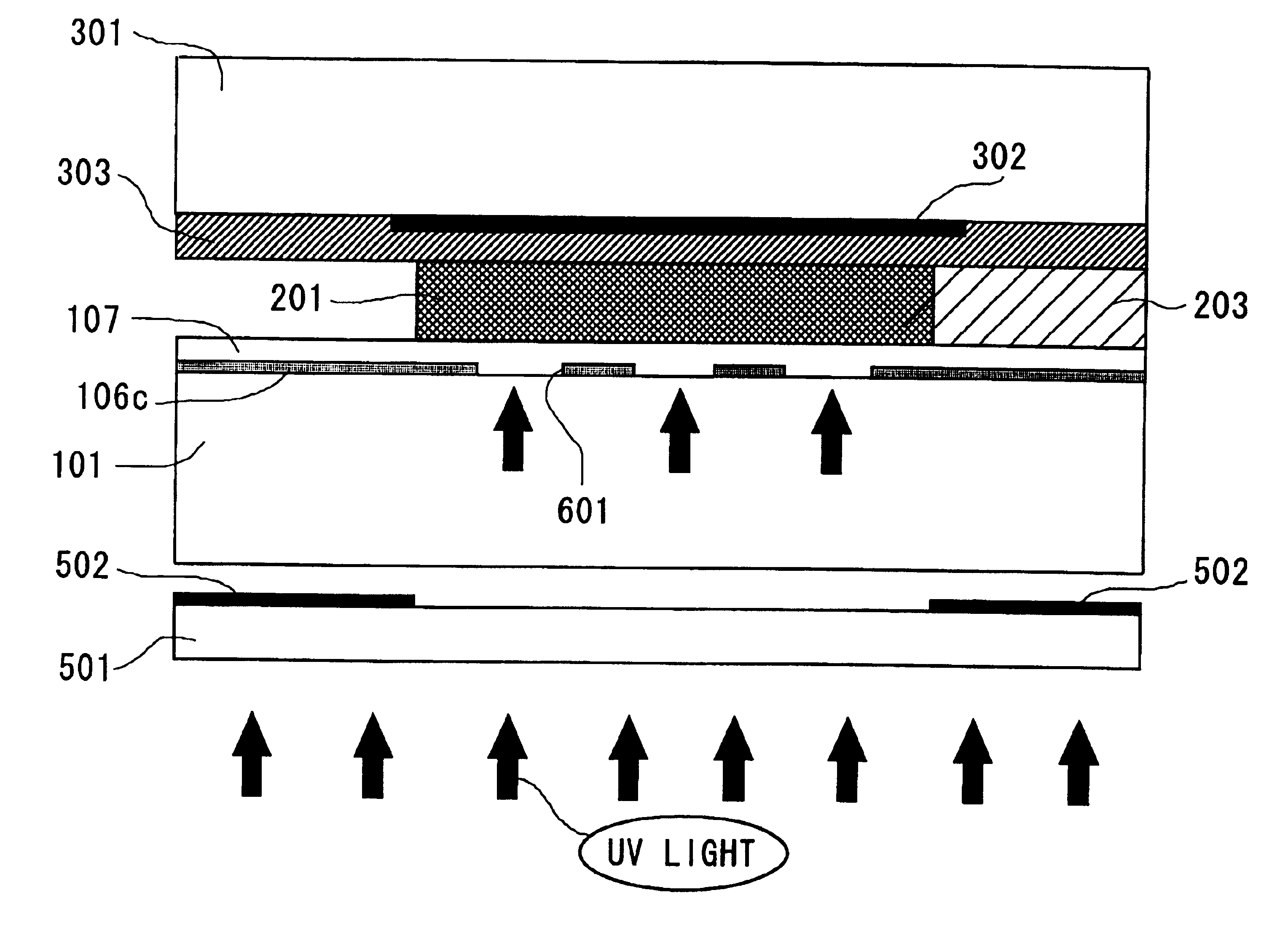
[0134]As shown in FIGS. 5 and 6, the LCD panel of the LCD device according to the first embodiment comprises a rectangular lower substrate 101, a rectangular upper substrate 301, and a liquid crystal layer 203 sandwiched by the substrates 101 and 301. The lower substrate 101 is coupled with the upper substrate 301 with the sealing member 201 in such a way that a small gap is formed between the substrates 101 and 301, as shown in FIG. 6. Liquid crystal is filled into the gap and confined by the member 201, forming the liquid crystal layer 203.

[0135]The surface of the lower substrate 101 is divided into a rectangular display area 401 located in the middle part, a rectangular-frame-shaped peripheral area 402 located in the periphery of the substrate 101 to surround the area 401, and a re...

second embodiment

[0167]FIG. 13 shows a LCD device according to a second embodiment of the invention, in which the same reference numerals are attached to the same elements as those of the first embodiment. Therefore, the explanation about the same configuration is omitted for FIG. 13 shows the same cross-section as FIG. 12. As seen from FIG. 13, an opposite light-blocking member 302A is formed to extend along the sealing member 201 in the periphery of the upper substrate 301. Thus, the member 302A is rectangular-frame shaped. The opposite common electrode 303 is formed on the substrate 301 to cover the member 302. The lattice-shaped black matrix (not shown) is formed on the substrate 301 within the area that is surrounded by the member 302 and opposite to the display area 401 of the lower substrate 101. The member 302A is opposite to the light-blocking members 106 of the lower substrate 101. The members 106 have the same structure as the light-blocking members 106a, 106b, and 106c of the first embod...

third embodiment

[0175]FIG. 14 shows a LCD device according to a third embodiment of the invention, in which the same reference numerals are attached to the same elements as those of the first embodiment. Therefore, the explanation about the same configuration is omitted for simplification.

[0176]FIG. 14 shows the same plan view as shown in FIG. 9. As seen from FIG. 9, a vernier 108 is provided by penetrating holes 108a and 108b of the light-blocking member 106. The holes 108a and 108b are located to overlap with the sealing member 201. The holes 109a are strip shaped and arranged in a direction at equal intervals, forming a scale. The holes 108b are formed to write specific numbers (e.g., 0 and 1) or signs (e.g., + and −). The holes 108a and 108b are used to efficiently irradiate the UV light to the sealing member 201 by way of the light-blocking members 106.

[0177]The vernier 108 is used to check the width of the UV-setting resin for the sealing member 201 written on the lower substrate 101 and / or t...


PUM

PropertyMeasurementUnit
heightaaaaaaaaaa
widthaaaaaaaaaa
temperatureaaaaaaaaaa

Abstract

A LCD device that receives curing light sufficiently to thereby realize approximately uniform curing of the material of the sealing member without eliminating the conductive light-blocking members. A first substrate has a display area and a peripheral area located to surround the display area. The display area includes pixels arranged regularly. The peripheral area includes a sealing member, wiring lines connected to the pixels, and conductive light-blocking members. A second substrate is coupled with the first substrate. A liquid crystal layer is formed between the first and second substrates. The sealing member is formed to overlap with the wiring lines and the light-blocking members in such a way that a non-overlapping area of the sealing member with the wiring lines and the light-blocking members is equal to 25% per unit area of the sealing member or greater.

Description

BACKGROUND OF THE INVENTION[0001]1. Field of the Invention[0002]The present invention relates to a Liquid-Crystal Display (LCD) device. More particularly, the invention relates to a LCD device formed by dripping a liquid crystal onto the lower substrate and by coupling it with the upper substrate with a sealing member, and a method of fabricating the device.[0003]2. Description of the Related Art[0004]As the methods of fabricating LCD devices, the “vacuum injection” method and the “dripping and coupling” method have been known so far.[0005]With the “vacuum injection” method, a pair of substrates (i.e., the lower and upper substrates) are coupled together with a sealing member with an injection hole in such a way as to form a gap therebetween. The sealing member is formed by a thermosetting resin. Thereafter, the substrates thus coupled are subjected to heat treatment for curing the member, forming a vacant cell. Then, the inside of the cell is degassed and immersed into a desired li...

Claims


Application Information

Patent Timeline
Patent Type & Authority Patents(United States)
IPC IPC(8): G02F1/1335G02F1/13G02F1/1339G02F1/1333
CPCG02F1/133512G02F1/1339G02F2202/023G02F2001/133388G02F1/133388
Inventor WATANABE, MAKOTOKADOTANI, TSUTOMUSASAKI, TAKESHIMATSUMOTO, KIMIKAZU
Owner GOLD CHARM LTD
Why Eureka
Try Eureka