Stacked microelectronic assemblies and methods of making same

a microelectronic assembly and stacking technology, applied in the direction of printed circuits, semiconductor devices, semiconductor/solid-state device details, etc., can solve the problems of chip dissipation of electrical power, cost and reliability problems, and the approach offers only limited reduction of the aggregate area of the circuit panel occupied, so as to facilitate the testing of individual subassemblies and compact structure

Inactive Publication Date: 2005-04-26
TESSERA INC
View PDF122 Cites 79 Cited by
  • Summary
  • Abstract
  • Description
  • Claims
  • Application Information

AI Technical Summary

Benefits of technology

[0017]Yet another aspect of the invention provides a stacked microelectronic assembly that includes a first subassembly, comprising a first microelectronic element and a first dielectric element, and a second subassembly, comprising a second microelectronic element and a second dielectric element. The first and second subassemblies are electrically interconnected with each other and arranged in a stacked arrangement relative to each other. The first dielectric element includes a plurality of terminals and first lands exposed on a surface that is opposite the surface that confronts the first microelectronic element. The second dielectric element has second lands exposed on a surface of the second dielectric element that is opposite the surface that confronts the second microelectronic element. The first and second subassemblies are arranged so that the respective land-bearing surfaces of the dielectric elements confront each other with the first lands overlying the second lands and being electrically connected thereto. Joining units connected to at least some of the terminals of the first subassembly project beyond the second subassembly. Preferably, the terminals of the first subassembly are disposed within a peripheral region of a dielectric element and the lands disposed within a central region, more preferably underlying the first microelectronic element. The lands of the first or second subassemblies are movable with respect to the respective microelectronic elements. As further explained below, preferred assemblies according to this aspect of the invention provide a relatively compact structure and also facilitate testing of the individual subassemblies prior to joining of the subassemblies.

Problems solved by technology

However, this approach suffers from cost and reliability problems.
This approach offers only limited reduction in the aggregate area of the circuit panel occupied by the chips.
Chips dissipate electrical power as heat during operation.
Where chips are stacked one atop the other, it is difficult to dissipate the heat generated by the chips in the middle of the stack.
Also, chips and circuit panels undergo substantial thermal expansion and contraction during operation.
Differences in thermal expansion and contraction can impose significant mechanical strain on elements of the assembly, including the electrical connections.

Method used


Image

  • Stacked microelectronic assemblies and methods of making same
  • Stacked microelectronic assemblies and methods of making same
  • Stacked microelectronic assemblies and methods of making same

Examples


Embodiment Construction

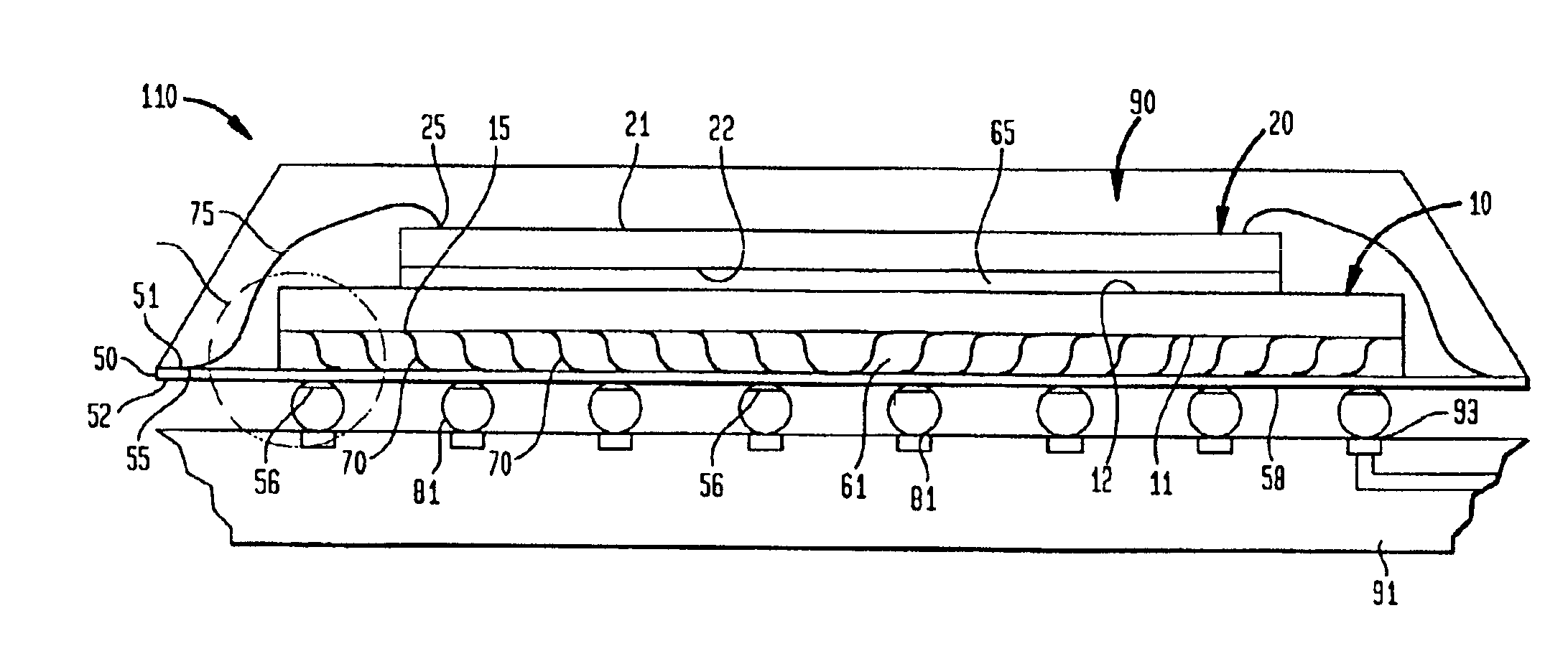
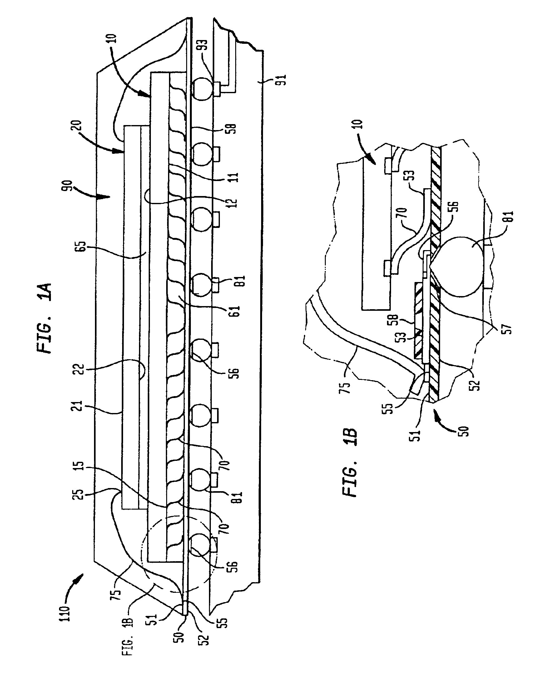
[0028]As shown in FIG. 1, a stacked microelectronic assembly 110 according to one embodiment of the present invention includes a first microelectronic element 10 and a second microelectronic element 20. Microelectronic element 10 has a face surface 11 and a back surface 12 opposite the face surface. Electrical contacts 15 are exposed on face surface 11. Microelectronic element 20 is arranged similarly to microelectronic element 10, in that it has face surface 21, a back surface 22 opposite the face surface and electrical contacts 25 are exposed on face surface 21. In the embodiment of FIG. 1, each microelectronic element 10 and 20 is a conventional semiconductor chip. The contacts 15 on the first microelectronic element are disposed in a “area array” or array of contacts at substantially equal distances over the area of face surface 11, whereas the contacts 25 are disposed in two rows adjacent opposite edges of such surface.

[0029]The assembly also includes a dielectric element 50 ha...


PUM


Abstract

A stacked microelectronic assembly includes a dielectric element and a first and second microelectronic element stacked one atop the other with the first microelectronic element disposed between the second microelectronic element and the dielectric. The dielectric element has opposed first and second surfaces with conductive features exposed at the first surface and terminals exposed on the second surface. Preferably, the contact-bearing face of the first microelectronic element confronts the first surface of the dielectric with at least some of the conductive features being movable with respect to the contacts or terminals. By providing such movable features, joining units have heights of about 300 microns or less may be joined to the terminals thereby reducing the overall height of the microelectronic assembly to 1.2 mm and less.

Description

CROSS-REFERENCE TO RELATED APPLICATIONS[0001]The present application claims benefit of U.S. Provisional Patent Application No. 60 / 261,059 filed Jan. 11, 2001, the disclosure of which is incorporated by reference herein.BACKGROUND OF THE INVENTION[0002]The present invention relates to stacked microelectronic assemblies and methods of making such assemblies, to methods of forming such assemblies and to components useful in such assemblies.[0003]Semiconductor chips are commonly provided as individual, prepackaged units. A standard chip has a flat, rectangular body with a large front face having contacts connected to the internal circuitry of the chip. Each individual chip typically is mounted in a package, which in turn is mounted on a circuit panel such as a printed circuit board and which connects the contacts of the chip to conductors of the circuit panel. In many conventional designs, the chip package occupies an area of the circuit panel considerably larger than the area of the ch...

Claims


Application Information

Patent Timeline
Patent Type & Authority Patents(United States)
IPC IPC(8): H01L25/065H01L23/49H01L23/28H01L23/31H01L23/48
CPCH01L23/3114H01L23/3128H01L24/10H01L24/50H01L25/0657H01L24/13H01L24/48H01L2224/13099H01L2224/32145H01L2224/48091H01L2224/48247H01L2225/0651H01L2225/06527H01L2225/06555H01L2225/06562H01L2225/06579H01L2225/06582H01L2924/01322H01L2924/15311H01L2224/4824H01L2924/01005H01L2924/01006H01L2924/01033H01L2924/014H01L2224/50H01L2224/73215H01L2224/32225H01L2224/48227H01L2224/73265H01L2224/0401H01L2224/06135H01L2224/06136H01L2924/00014H01L2924/00H01L2924/00012H01L24/73H01L2224/02379H01L2224/13H01L2224/45014H01L2224/85205H01L2224/85207H01L2924/181H01L2224/45015H01L2924/207H01L2924/206
Inventor DAMBERG, PHILIPMITCHELL, CRAIG S.RILEY, JOHN B.WARNER, MICHAELFJELSTAD, JOSEPH
Owner TESSERA INC
Why Eureka
Try Eureka