

Electro-optical apparatus, matrix substrate, and electronic unit
a technology of optical apparatus and matrix substrate, applied in the direction of identification means, coupling device connections, instruments, etc., can solve the problems of increasing the resistance of the common electrode, the failure to supply sufficient current to the central part of the screen, and the increase of the voltage drop in pixels, so as to reduce the resistance of the second electrode layer, reduce the width of the display panel frame, and raise the aperture ratio
- Summary
- Abstract
- Description
- Claims
- Application Information
AI Technical Summary
Benefits of technology
Problems solved by technology
Method used
Image

Examples
first exemplary embodiment
[First Exemplary Embodiment]
[0046]The exemplary embodiment is illustrated below with reference to the drawings.
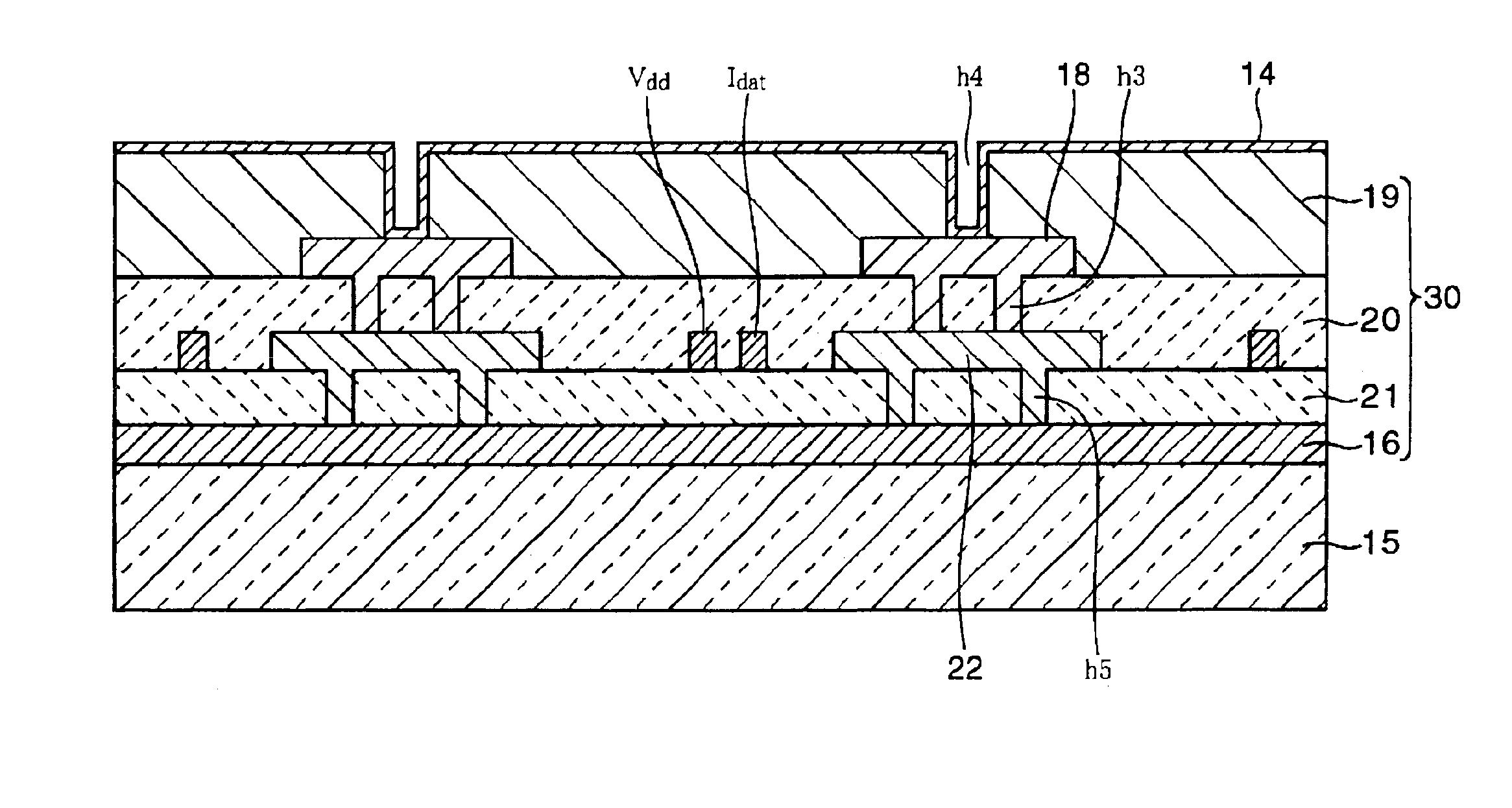
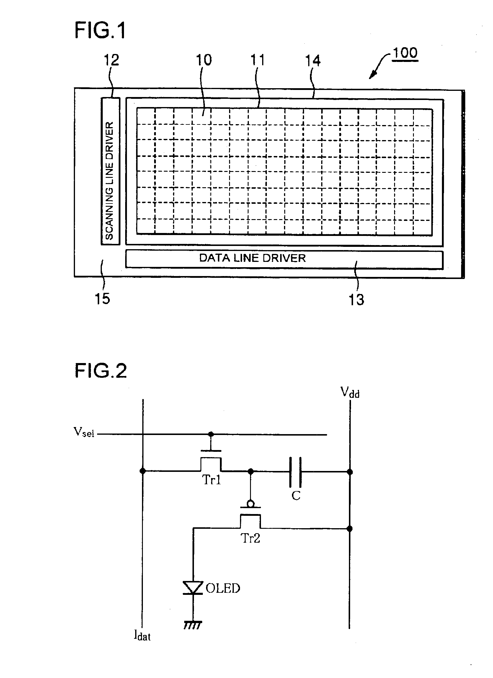
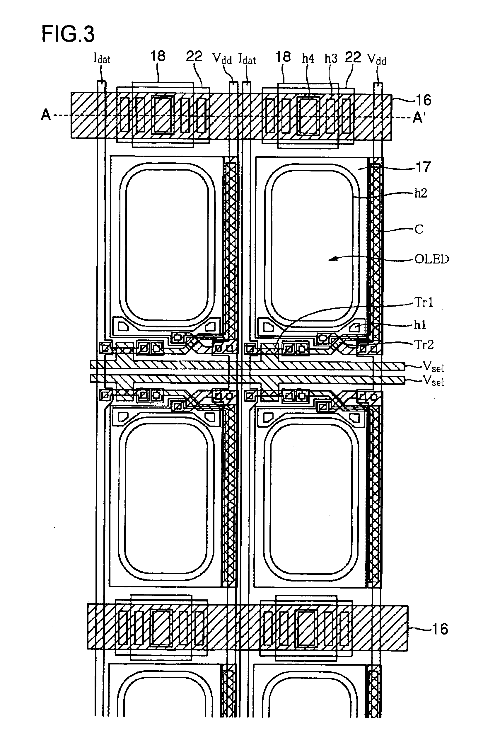
[0047]FIG. 1 is a schematic of an active-matrix-type organic EL display panel 100 of the exemplary embodiment. As illustrated in FIG. 1, a plurality of pixels 10, a scanning line driver 12, and a data line driver 13 are disposed on or above a substrate 15. The plurality of pixels 10 have laminated structures disposed on a display area 11. The scanning line driver 12 outputs scanning signals to scanning lines, which are disposed in a row direction and connected to a group of the pixels 10. The data line driver 13 supplies data signals and power supply voltages to data lines and power supply lines, respectively. The data lines and the power supply lines are disposed in a column direction and connected to a group of the pixels 10. The pixels 10 form an N-row, M-column pixel matrix, in which the row direction and the column direction are disposed orthogonally and form a pixel m...
second exemplary embodiment
[Second Exemplary Embodiment]
[0058]FIG. 5 shows the layout of wiring in an organic EL display panel 100 according to a second exemplary embodiment of the present invention. This exemplary embodiment differs from the first exemplary embodiment on the point of that auxiliary cathode wiring 16 is disposed in the column direction. Referring to FIG. 5, where one pixel includes three RGB picture elements, three auxiliary cathode wiring 16 are spaced uniformly every two pixels in the column direction. Two data lines Idat are disposed at two sides of each auxiliary cathode wiring 16. Between adjacent auxiliary cathode wiring 16, two power supply lines Vdd are formed as a pair. The sum of the widths of the one auxiliary cathode wiring 16 and the two data lines Idat is substantially equal to the sum of the widths of the pair of power supply lines Vdd. Thereby, the layout of the wiring shown in this figure is arranged so as to have symmetry about any column. On the other hand, in the row direc...
third exemplary embodiment
[Third Exemplary Embodiment]
[0062]FIG. 7 shows the layout of wiring in an organic EL display panel 100 according to a third exemplary embodiment of the present invention. This exemplary embodiment differs from the first and second exemplary embodiments on the point of that auxiliary cathode wiring 16 are disposed in both the row and the column directions. For the sake of distinguishing between the auxiliary cathode wiring 16 which are disposed in both the row and the column directions, the auxiliary cathode wiring 16 disposed along the row direction are called first auxiliary cathode wiring 16-1, while the auxiliary cathode wiring 16 disposed along the column direction are called second auxiliary cathode wiring 16-2. When the “auxiliary cathode wiring 16” is simply used, it includes both. Referring to FIG. 7, where one pixel consist of three RGB picture elements, three second auxiliary cathode wiring 16-2 are spaced uniformly every two pixels in the column direction. Two data lines ...
PUM
 Abstract
Description
Claims
Application Information