Electrooptic device and electronic apparatus

a technology of electronic equipment and optical components, applied in the field of optical components, can solve the problems of non-display regions, i.e., picture frame regions, liquid crystal devices may not be disposed at the center, and the liquid crystal device may not be manufactured, so as to achieve the effect of preventing the manufacture of liquid crystal devices, reducing wiring resistance, and maintaining display quality at a higher level

Inactive Publication Date: 2005-05-03
SEIKO EPSON CORP
View PDF21 Cites 44 Cited by
  • Summary
  • Abstract
  • Description
  • Claims
  • Application Information

AI Technical Summary

Benefits of technology

[0041]The electrooptic device provided with the shading layer may further comprise a color layer containing at least two different colors; and a member defining the two colors; wherein the member may comprise substantially the same material as that for the shading layer. Accordingly, a method for manufacturing a liquid crystal device can be prevented from being complicated.
[0042]In the electrooptic device having the structure described above, the wires may comprise a first conductive film having a resistance lower than that of the first electrode. According to this structure, the wiring resistance is decreased, and hence, the display quality can be maintained at a higher level.

Problems solved by technology

However, in the structure described above, a region on which the driver IC is mounted is necessary for each substrate, and hence, there has been a problem in that a non-display region, i.e., a picture frame region, of a liquid crystal device becomes larger.
In addition, since a shape having a protruding portion which largely protrudes from one of the left side and the right side of the liquid crystal device or one of the upper side and the lower side thereof, that is, an asymmetrical shape, is formed, when this liquid crystal device is contained in a container of a portable electronic apparatus, for example, there has been a problem in that the liquid crystal device may not be contained in the container unless otherwise the peripheral portion thereof for the electronic apparatus is increased, or in addition, the liquid crystal display portion may not be disposed at the center of the electronic apparatus.
However, the conventional liquid crystal device 150 having the structure described above has the following problems.
As described above, in order to provide the vertical conduction members 142, since only limited spaces of the left and the right of the lower side of the upper substrate 101 can be used, when a number of the wires 140 and 143 are disposed, pitches between the wires 140 and between the wires 143 (that is, the wire width + the gap between the wires) must be decreased, and as a result, there has been a problem in that short-circuiting may occur between adjacent wires, or that the reliability of the wires may be degraded in some cases.
When the wires 140 and 143 are provided outside the sealing material 141 as described above, and the number of wires is increased, the region in which the wires are formed is increased, and as a result, it becomes difficult to produce liquid crystal devices having a smaller picture frame.
In order not to increase the regions in which wires are formed even when the display capacity of liquid crystal devices is increased, it has been considered that the pitches between the wires are decreased, that is, the wire width is decreased and / or the gap between the wires is decreased; however, in the case described above, the resistance of the wire is increased, and as a result, the display quality of the liquid crystal device may be adversely affected in some cases.
The resistance of the wires formed of a conventional wire material is increased to the range of from several thousand ohms to several mega ohms, and thus a problem of deformed signal waveforms or the like may arise in some cases.

Method used


Image

  • Electrooptic device and electronic apparatus
  • Electrooptic device and electronic apparatus
  • Electrooptic device and electronic apparatus

Examples


first embodiment

of Electrooptic Device

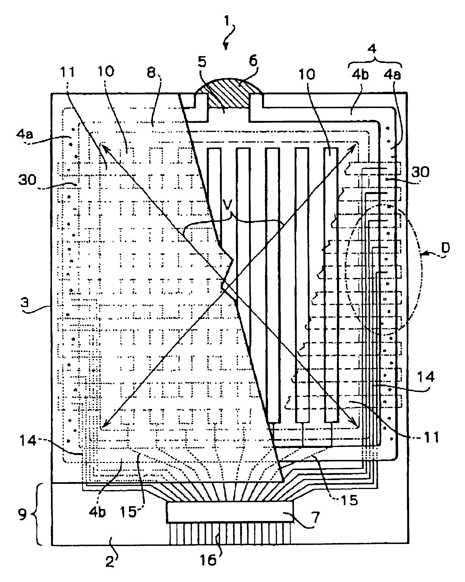
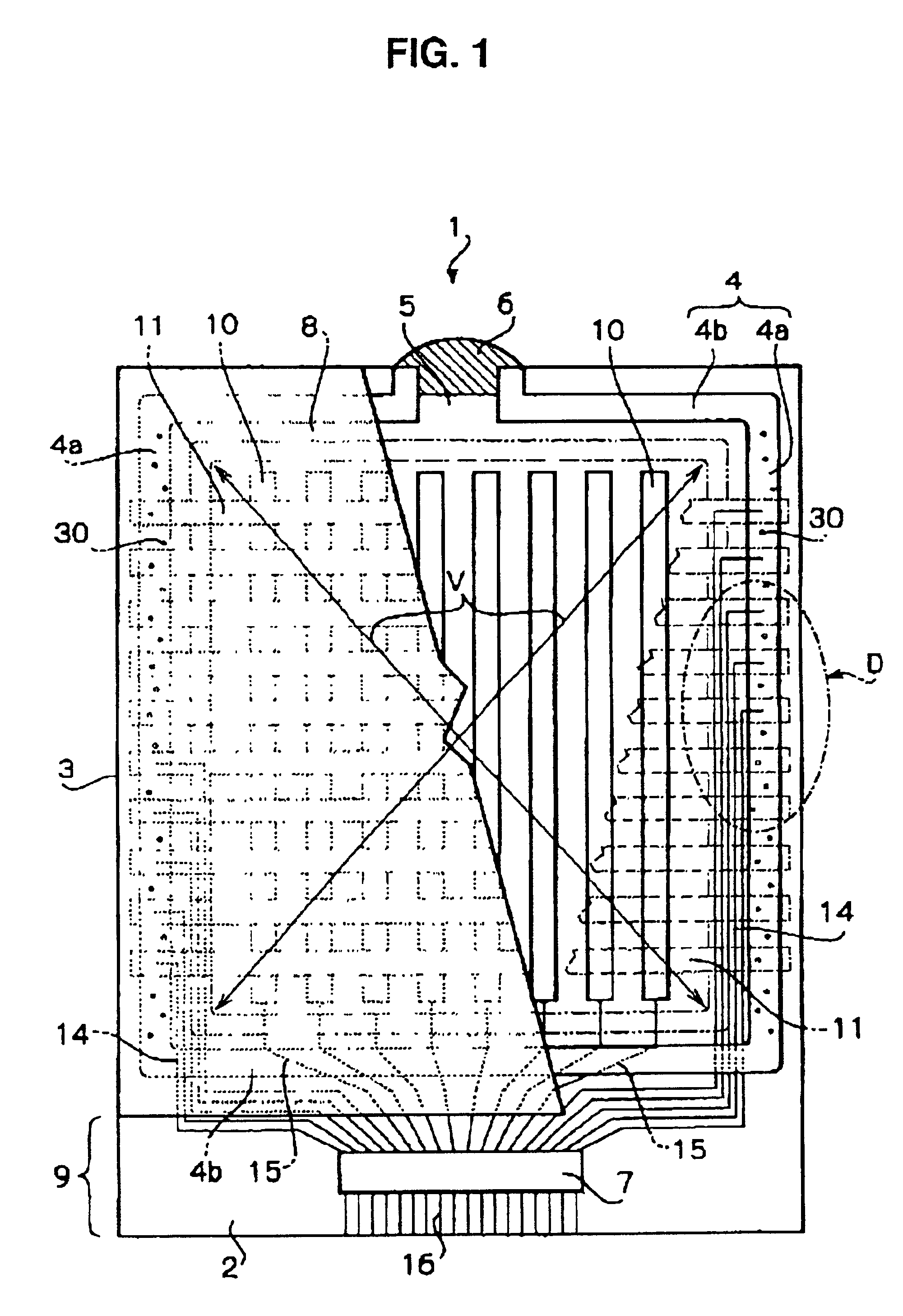
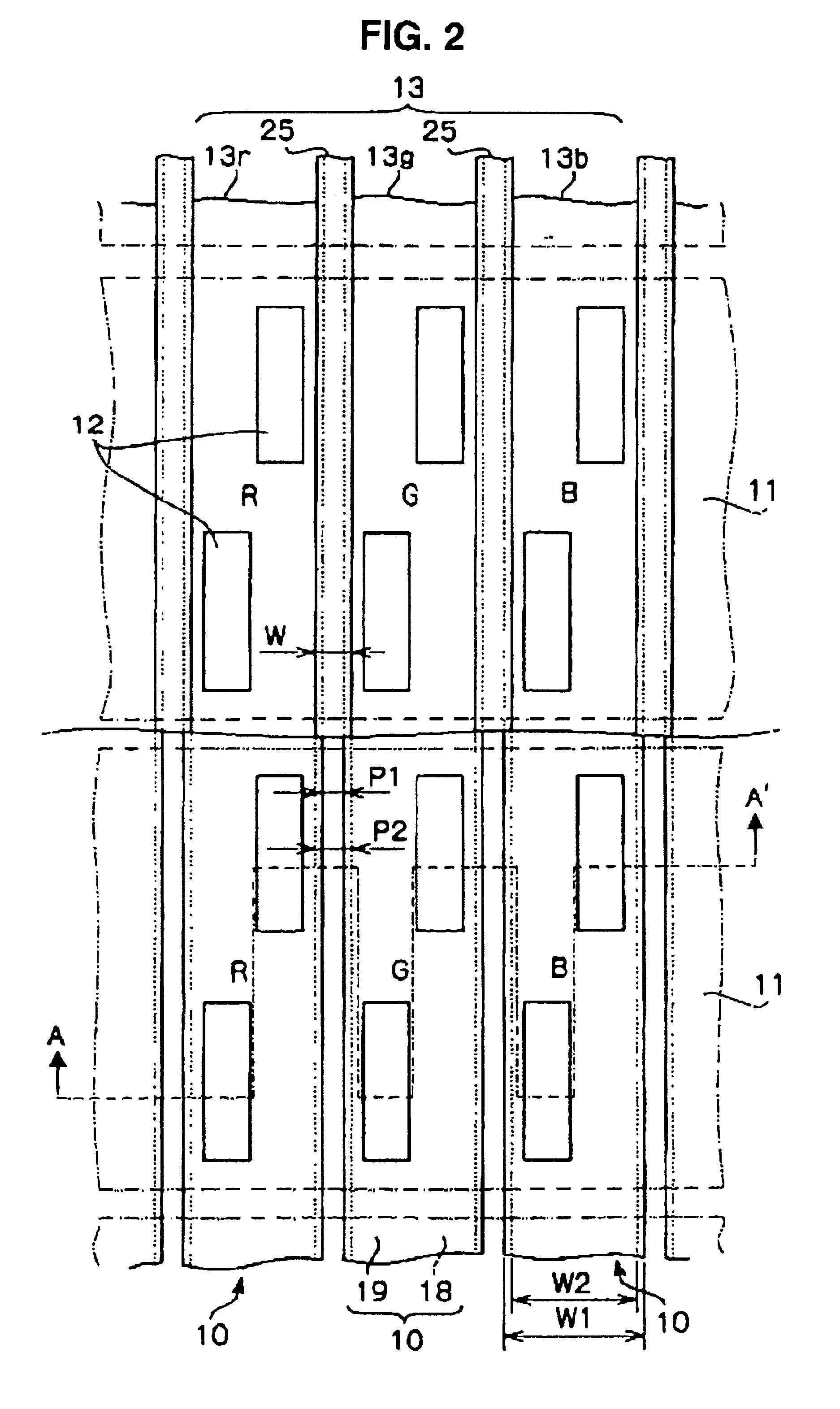
[0094]Hereinafter, an embodiment in which the present invention is applied to a liquid crystal device, which is a passive matrix type, is a transflective type, and performs color display, will be described. FIG. 1 shows the plan structure of a liquid crystal device according to an embodiment of an electrooptic device of the present invention. In addition, FIG. 2 is an enlarged plan view showing pixel portions of the liquid crystal device in FIG. 1. In addition, FIG. 3 shows the cross-sectional structure of the liquid crystal device taken along the line A-A′ in FIG. 2. FIG. 4 shows an enlarged vertical conduction member indicated by the arrow D in FIG. 1. Furthermore, FIG. 5 shows the cross-sectional structure of a sealing portion taken along the line B-B′ in FIG. 4. In all the figures described below, in order to facilitate understanding of the structure of the liquid crystal device, the thicknesses and the dimensional ratios of individual constituent elements ...

second embodiment

of Electrooptic Device

[0135]FIGS. 6 and 7 each show a major portion of a liquid crystal device which is one example of an electrooptic device according to another embodiment of the present invention. In this embodiment, since the entire structure of the liquid crystal device is equivalent to that of the embodiment shown in FIG. 1, the detailed description is omitted. The point of this embodiment different from that of the above embodiment shown in FIGS. 4 and 5 is only the structure relating to the vertical conduction member, and this point will be described with reference to FIGS. 6 and 7. In this embodiment, the same reference numerals in FIGS. 4 and 5 designate the same constituent elements in FIGS. 6 and 7.

[0136]In the embodiment shown in FIG. 4, in the sealing material 4 formed continuously in a rectangular shape, the parts thereof along the right sides and the left sides of the substrates 2 and 3 are formed as the conductive sealing material 4a, and the parts along the upper s...

third embodiment

of Electrooptic Device

[0146]FIG. 9 shows a liquid crystal device which is one example of an electrooptic device according to still another embodiment of the present invention. In this embodiment, since the basic structure of a liquid crystal device 41 shown in this embodiment is equivalent to that of the embodiment shown in FIG. 1, the detailed description is omitted. The point of the liquid crystal device 41 different from the liquid crystal device 1 shown in FIG. 1 mainly relates to a method for disposing the wires, and this point will be described with reference to FIG. 9.

[0147]In the liquid crystal device 1 in FIG. 1, of a plurality of the common electrodes 11, concerning the common electrodes 11 in the upper half, the wires 14 extend from the right sides thereof, and on the other hand, concerning the common electrodes 11 in the lower half, the wires 14 extend from the left sides thereof. In contrast, in the liquid crystal device 41 shown in FIG. 9, the common electrode 11 locat...


PUM

PropertyMeasurementUnit
resistanceaaaaaaaaaa
diameteraaaaaaaaaa
widthaaaaaaaaaa

Abstract

A liquid crystal device 1, that is, an electrooptic device, has a second electrode 11 provided so as to oppose a first electrode 10, and a liquid crystal provided between the first electrode 10 and the second electrode 11. This liquid crystal device 1 further has a first substrate 2 on which the first electrode 10 is provided and a wire 14 which is formed on the first substrate 2 and is electrically connected to the second electrode 11 at a conduction position 4a. Since the wire 14 extends inside the conduction position 4a, the picture frame region that is outside a sealing material 4 can be decreased.

Description

FIELD OF THE INVENTION[0001]The present invention relates to electrooptic devices, such as a liquid crystal device, an EL (Electro Luminescence) device, and an electrophoretic device, and relates to electronic apparatuses using these electrooptic devices.DESCRIPTION OF THE RELATED ART[0002]In recent years, in electronic apparatuses such as notebook personal computers, mobile phones, wristwatches, and the like, liquid crystal devices have been widely used as means for displaying various information. In addition, it is expected that EL devices will also be used in the future. In electronic apparatuses, specifically in portable type electronic apparatuses, such as notebook personal computers, mobile phones, wristwatches, and the like, a liquid crystal device or the like is contained in a limited space inside the case. However, according to demands to increase the amount of information which can be displayed by the liquid crystal device or the like, it has been desired that the display ...

Claims


Application Information

Patent Timeline
Patent Type & Authority Patents(United States)
IPC IPC(8): G02F1/13G02F1/1339G02F1/1345H01L27/32H01L27/28H01L51/52H01L51/50G02F1/1365G09F9/00G09F9/30
CPCG02F1/1339G02F1/1345H01L27/3211G02F2001/13456H01L51/5246H01L27/322H01L27/3276H01L27/3288G02F1/13456H10K59/35H10K59/38H10K59/179H10K59/131H10K50/8426
Inventor HINATA, SHOJIARUGA, YASUHITOTSUYUKI, TADASHI
Owner SEIKO EPSON CORP
Why Eureka
Try Eureka