Exposure apparatus and exposure method

a technology of exposure apparatus and exposure method, which is applied in the field of exposure apparatus, can solve the problem that the integrated exposure amount of a wafer cannot be constant, and achieve the effect of accurate control of the integrated exposure amoun

Inactive Publication Date: 2005-05-03
CANON KK
View PDF6 Cites 7 Cited by
  • Summary
  • Abstract
  • Description
  • Claims
  • Application Information

AI Technical Summary

Benefits of technology

[0006]It is accordingly an object of the present invention to provide an exposure apparatus, an exposure method or a device manufacturing method, by which any influence of reflection light from a reticle is removed or reduced such that accurate control of the integrated exposure amount can be accomplished.

Problems solved by technology

Such a technique, however, involves a problem that, even if the control is made to keep the output of the photodetector constant, the integrated exposure amount of a wafer cannot be made constant.

Method used


Image

  • Exposure apparatus and exposure method
  • Exposure apparatus and exposure method
  • Exposure apparatus and exposure method

Examples


Embodiment Construction

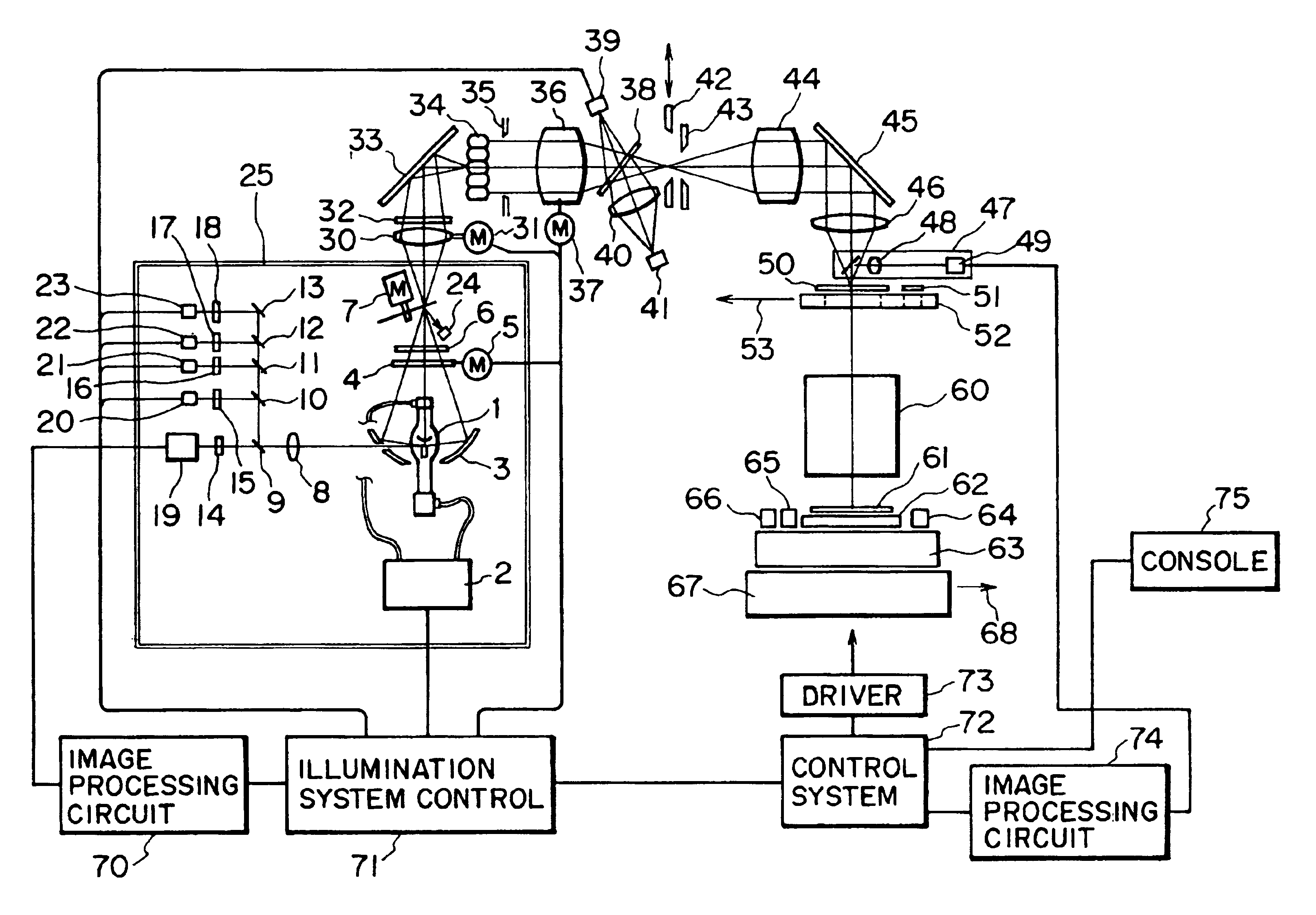
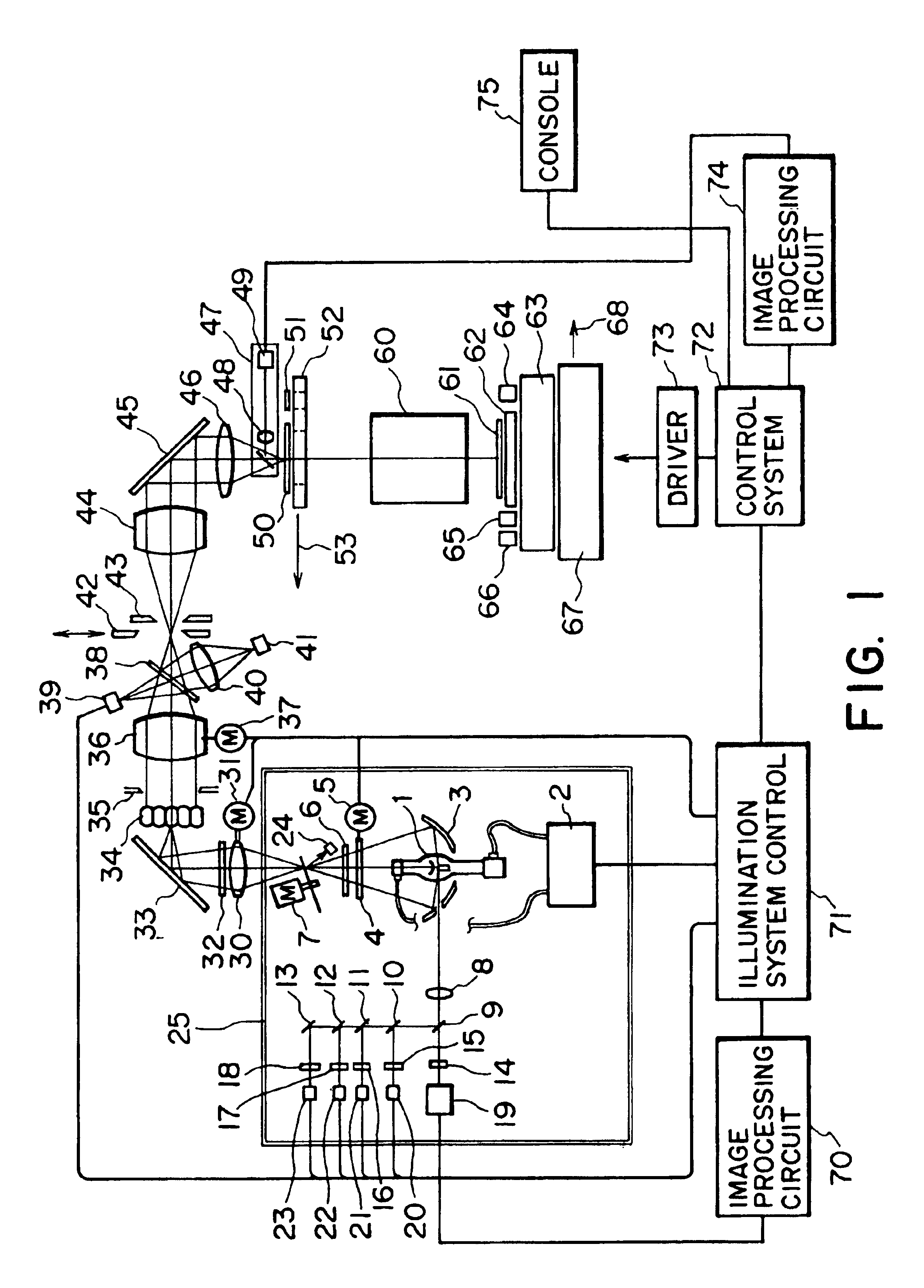
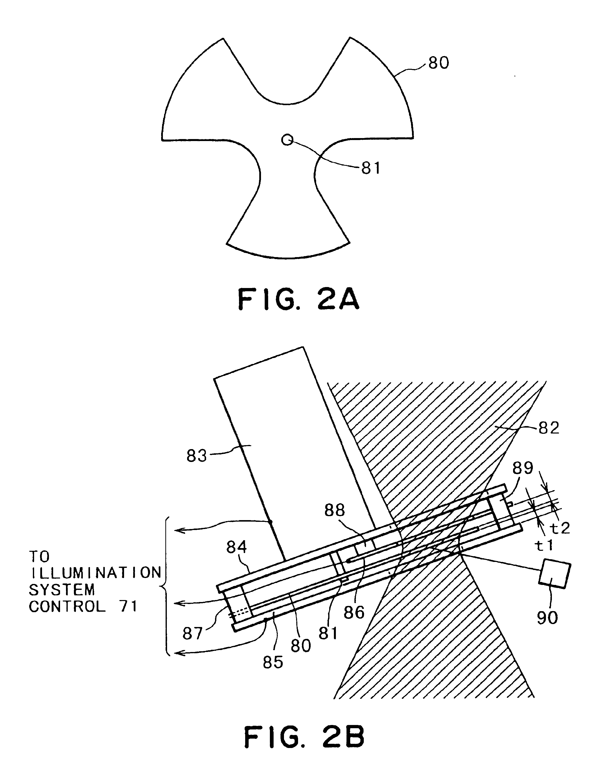
[0024]In an exposure apparatus and an exposure method according to preferred embodiments of the present invention, a pattern of an original (reticle), as illuminated by an illumination optical system for illuminating the original with exposure light, is projected and printed on a substrate (wafer) through a projection optical system, wherein an output of a light source is controlled on the basis of an output of a photodetector disposed at a position which is optically conjugate with the pattern surface of the original. Specifically, any influence of reflection light from the pattern surface of the original is removed or reduced on the basis of an output of the photodetector produced as the pattern surface of the original is illuminated by the illumination optical system.

[0025]Such exposure apparatus and exposure method may be a scan type exposure apparatus and a scan type exposure method in which the exposure is performed while the original and the substrate are scanningly moved rel...


PUM

PropertyMeasurementUnit
widthaaaaaaaaaa
long-wavelength interceptingaaaaaaaaaa
i-line wavelengthaaaaaaaaaa

Abstract

A scan type exposure apparatus wherein a pattern of an original is lithographically transferred to a substrate sequentially while the original and the substrate are scanningly moved relative to exposure light, the apparatus including a photodetector disposed at a position optically conjugate with the original, and a storing device for storing correction information with respect to an output of the photodetector, in relation to different positions of the original to be illuminated with the exposure light, such that, in the lithographic pattern transfer, the output of the photodetector can be corrected by use of the correction information.

Description

FIELD OF THE INVENTION AND RELATED ART[0001]This invention relates to an exposure apparatus such as a semiconductor exposure apparatus of scan type, for example, and an exposure method and a device manufacturing method to be used therewith. More particularly, the invention is concerned with an exposure apparatus and an exposure method in which any influence of reflection light from a reticle or a wafer, for example, is removed by which accurate control of integrated exposure amount is enabled[0002]Scan type exposure apparatuses are known as an apparatus for manufacture of semiconductor devices, in which a pattern of a reticle is lithographically transferred onto a wafer through a scanning operation FIG. 13 is a schematic view of a main portion of an ordinary scan type semiconductor exposure apparatus. In this apparatus, as shown in the drawing, a portion of a pattern 200 formed on a reticle 50 is illuminated with slit-like illumination light 201, by use of a continuous emission ligh...

Claims


Application Information

Patent Timeline
Patent Type & Authority Patents(United States)
IPC IPC(8): G03F7/20H01L21/027
CPCG03F7/70066G03F7/70941G03F7/70558G03F7/70358
Inventor SATO, MITSUYA
Owner CANON KK
Why Eureka
Try Eureka