Method and apparatus for adjusting characteristics of electron source, and method for manufacturing electron source

a technology of electron source and characteristic adjustment, which is applied in the field of method and apparatus for adjusting characteristics of electron source, and the method for manufacturing electron source, can solve the problems of complex management of manufacturing processes, complex adjustment methods, and complex apparatus structure and cos

Inactive Publication Date: 2005-05-10
CANON KK
View PDF18 Cites 15 Cited by
  • Summary
  • Abstract
  • Description
  • Claims
  • Application Information

AI Technical Summary

Benefits of technology

[0012]An object of the present invention is to provide a method and an apparatus for adjusting characteristics, and a method for manufacturing an electron source, the methods and the apparatus making the characteristics of a multi-electron source to be almost the same in a simple process by the use of properties peculiar to an electron-emitting device.

Problems solved by technology

Consequently, the adjustment method becomes complicated.
And if an adjustment apparatus is made in accordance with the adjustment method, the apparatus becomes complicated in structure and high in cost.
And further, in a manufacturing method of an electron source incorporating the adjustment method as a part of the processes thereof, the adjustment method is a primary factor of making the management of manufacturing processes complicated.

Method used


Image

  • Method and apparatus for adjusting characteristics of electron source, and method for manufacturing electron source
  • Method and apparatus for adjusting characteristics of electron source, and method for manufacturing electron source
  • Method and apparatus for adjusting characteristics of electron source, and method for manufacturing electron source

Examples


embodiment 1

[Embodiment 1]

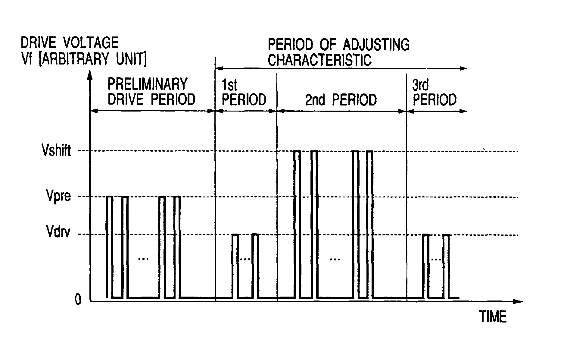
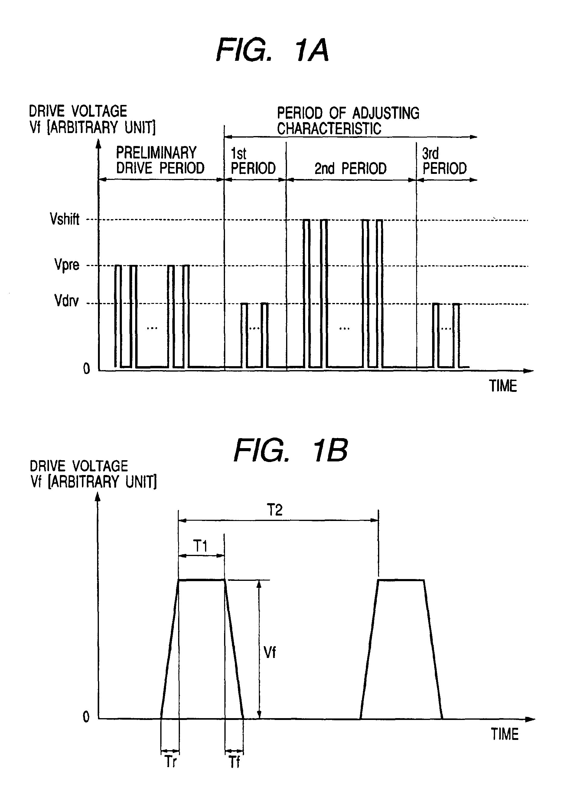
[0044]The present embodiment includes the process of preliminary drive processing capable of decreasing changes with the passage of time prior to the process of characteristic adjustment in its manufacturing process.

(Preliminary Drive Processing Process)

[0045]In case of a surface conduction electron-emitting device, for forming an electron-emitting region, the energization forming operation thereof is performed and carbon or a carbon compound is deposited at a part in the vicinity of the electron-emitting region by the energization activation operation thereof as the occasion demands. Moreover, it is preferable to execute a stabilization process after the completion of the energization activation operation. The process is one for removing organic materials in a vacuum chamber by exhausting them. It is preferable to use a vacuum pumping apparatus for exhausting the vacuum chamber that does not use any oil in order that organic materials such as oil to be generated from ...

embodiment 2

[Embodiment 2]

[0109]In the first embodiment, the procedure for performing the individual characteristic adjustment to every device of the electron-emitting devices in the display panel 301 has been described. On the contrary, in the present embodiment, the time spent for characteristic adjustment is not so much increased even in the case where the structure of the electron-emitting devices in the display panel 301 take a high density and the number of all of the electron-emitting devices is remarkably increased.

[0110]To put it concretely, the procedure of performing the characteristic adjustment of one device or a plurality of devices of the devices in the display panel 301 shown in FIG. 10 simultaneously and the configuration of an apparatus corresponding to the characteristic adjustment are described in the following. Incidentally, the concepts of the preliminary drive processing and the characteristic adjustment to one device are the same as that of the first embodiment.

[0111]FIG...


PUM


Abstract

A method for adjusting characteristics of an electron source having a plurality of electron-emitting devices, and a method for manufacturing the electron source include the step of applying a pulse of a voltage for adjustment to an electron-emitting device to be adjusted one or more times according to a characteristic of the electron-emitting device, wherein the voltage for adjustment is selected from a plurality of voltages having discrete values according to the characteristic of the electron-emitting device, and a number of applying times of the pulse is determined according to the characteristic of the electron-emitting device and the selected voltage.

Description

[0001]This application is a division of application Ser. No. 10 / 209,876, filed Aug. 2, 2002 now U.S. Pat. No. 6,712,660.BACKGROUND OF THE INVENTION[0002]1. Field of the Invention[0003]The present invention relates to a method and an apparatus for adjusting characteristics of an electron source equipped with many electron-emitting devices, and a method for manufacturing an electron source.[0004]2. Related Background Art[0005]Conventionally, two kinds of electron-emitting devices of a hot cathode device and a cold cathode device are known. As the cold cathode device of the two, for example, an electric field emission electron-emitting device (hereinafter referred to as an FE type), a metal / insulator-layer / metal electron-emitting device (hereinafter referred to as an MIM type), a surface conduction electron-emitting device (hereinafter referred to as a surface conduction emission device), and the like are known.[0006]In an electron source in which many electron-emitting devices are wir...

Claims


Application Information

Patent Timeline
Patent Type & Authority Patents(United States)
IPC IPC(8): H01J9/42G09G3/22G09G3/20
CPCH01J9/42G09G3/22G09G3/20
Inventor AOKI, SHUJIOGUCHI, TAKAHIRO
Owner CANON KK
Why Eureka
Try Eureka