Trench isolation employing a doped oxide trench fill

a technology of doped oxide and trench filling, which is applied in the manufacturing of semiconductor/solid-state devices, basic electric elements, electrical equipment, etc., can solve the problems of changing the characteristics of the device, increasing the aspect ratio, and unsuitable known methods, and achieves acceptable interface quality

Inactive Publication Date: 2005-05-10
IBM CORP +1
View PDF10 Cites 26 Cited by
  • Summary
  • Abstract
  • Description
  • Claims
  • Application Information

AI Technical Summary

Benefits of technology

[0012]The present invention provides an isolation trench in which a reflowed doped oxide material is employed to fill the trench in a void-free manner, a thin liner layer is used to line the walls and bottom of the trench and serves as an effective diffusion barrier for oxide dopants while being transparent to the mobile ions, and a thin capping layer is utilized to protect the doped oxide from wet etch treatments as well as to serve as a diffusion barrier. In addition, the thin liner has an acceptable interface quality (as determined by the interface density of states at silicon mid-gap energy) that is compatible with ultra-low leakage applications.

Problems solved by technology

As newer generations of semiconductor device features become increasingly smaller and the number of elements increased, these known methods are often unsuitable or are increasingly difficult to be manufactured in a controllable manner.
Further, three-dimensional (3D) integration of the devices requires even deeper isolation trenches, resulting in even higher aspect ratios.
The use of such doped oxides, however, has the disadvantage that dopants in the oxide, such as boron, arsenic, or phosphorus, may diffuse out of the doped oxide and into the device regions during the anneal step and other subsequent high temperature processing steps and change the characteristics of the devices.
Moreover, such doped oxides have the disadvantage of a high etch rate when exposed to wet solvents, such as acids, and thus cannot be etched in a readily controllable or repeatable manner.
Because current state-of-the-art fabrication processes use isolation trenches that are only 100 nm wide, substantial protection from dopant penetration is not practical when the reflowable material is a highly doped oxide.
Thus, the process is not suitable for trenches having increasingly smaller feature sizes (of about 120 nm or less) and higher aspect ratios (of about 5 or larger).

Method used


Image

  • Trench isolation employing a doped oxide trench fill
  • Trench isolation employing a doped oxide trench fill
  • Trench isolation employing a doped oxide trench fill

Examples


Embodiment Construction

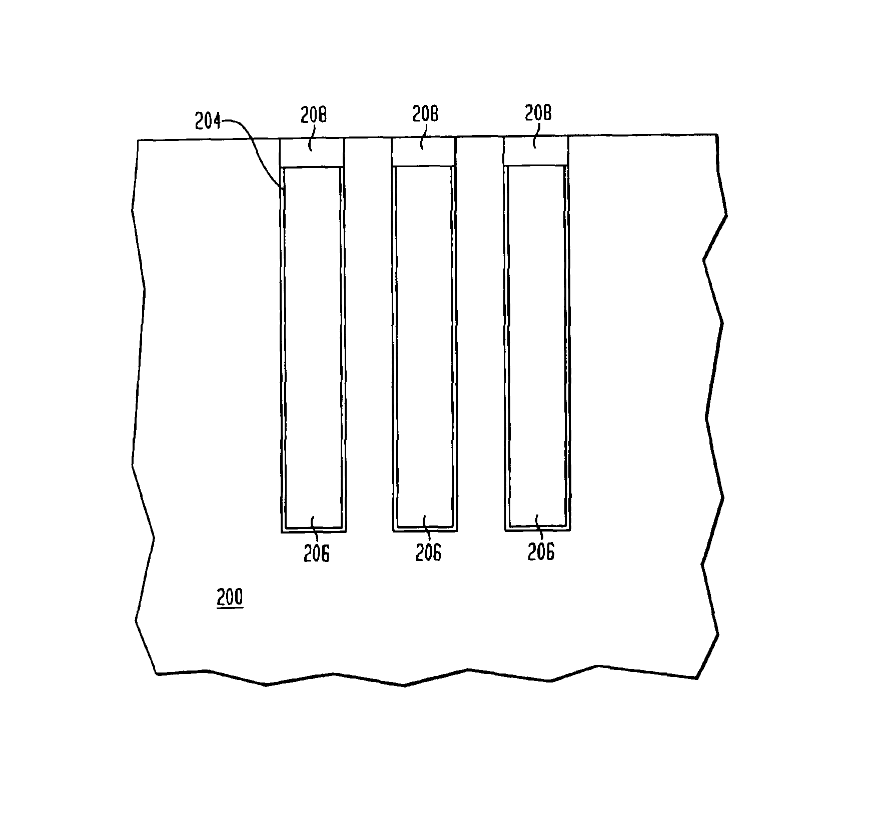
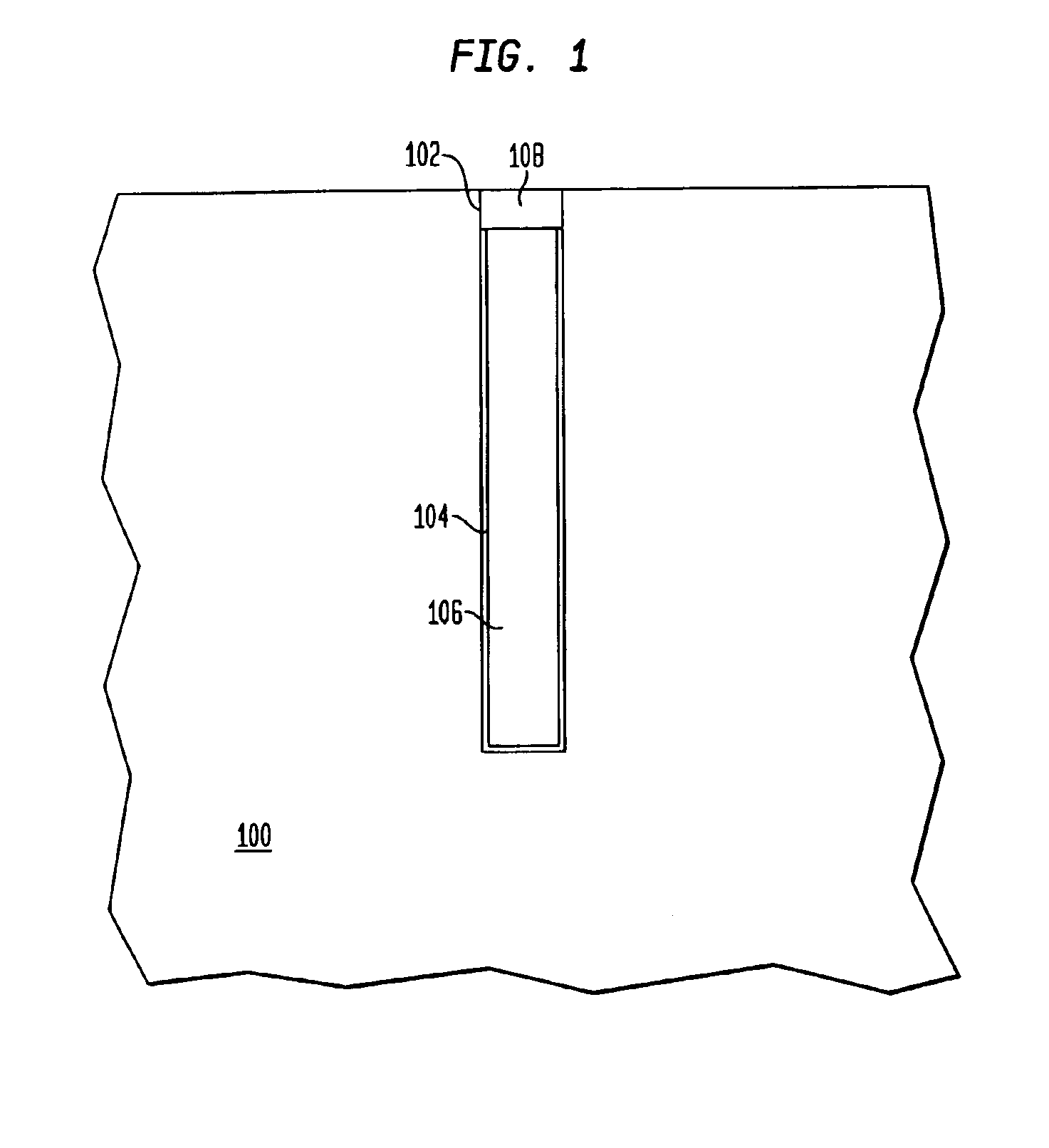
[0024]FIG. 1 shows a cross-sectional view of a portion of a substrate in which a trench structure is formed in accordance with the invention. A trench 102 having an aspect ratio of at least 5:1 is formed in a semiconductor substrate 100. The bottom and sidewalls of the trench 102, except for the uppermost portion of the trench, is lined with a thin liner material 104, which is typically a high-quality silicon oxide (SiO2) layer of about 100 Å thickness that is covered with an about 60-200 Å thick layer of silicon nitride (SiN).

[0025]The high-quality silicon oxide formed next to the substrate 100 ensures a low leakage (i.e., low trap generation) current of typically less than about 50 fA / μ2. To obtain such a low leakage current, a substantially good interface is needed between the substrate 100 and the liner 104. The interface quality is determined by measuring the density of mid-gap the energy states at the silicon interface which is an indication of the number of charge traps and / o...


PUM


Abstract

A trench isolation structure is formed in a substrate. One or more openings are formed in a surface of the substrate, and a liner layer is deposited at least along a bottom and sidewalls of the openings. A layer of doped oxide material is deposited at least in the openings, and the substrate is annealed to reflow the layer of doped oxide material. Only a portion near the surface of the substrate is removed from the layer of doped oxide material in the opening. A cap layer is deposited atop a remaining portion of the layer of doped oxide material in the opening.

Description

BACKGROUND OF THE INVENTION[0001]The present invention is directed to semiconductor integrated circuit devices and, more particularly, to processes for the fabrication of semiconductor integrated circuit devices that include isolation trenches for low leakage transistors.[0002]Various isolation methods have been employed to electrically isolate one or more semiconductor device elements formed in a substrate from other device elements. Such methods have included p-n junction isolation and localized oxidation of silicon (LOCOS). As newer generations of semiconductor device features become increasingly smaller and the number of elements increased, these known methods are often unsuitable or are increasingly difficult to be manufactured in a controllable manner. To isolate such smaller and more highly integrated semiconductor device elements, trench isolation is commonly employed in which a trench is formed in a semiconductor substrate and surrounds the region that is to be electrically...

Claims


Application Information

Patent Timeline
Patent Type & Authority Patents(United States)
IPC IPC(8): H01L21/762H01L21/70
CPCH01L21/76224
Inventor BELYANSKY, MICHAELKNORR, ANDREASGLUSCHENKOV, OLEGPARKS, CHRISTOPHER
Owner IBM CORP
Why Eureka
Try Eureka