Method of using tantalum-aluminum-nitrogen material as diffusion barrier and adhesion layer in semiconductor devices

a technology of tantalum-aluminum-nitrogen and diffusion barrier, which is applied in the direction of semiconductor devices, semiconductor/solid-state device details, electrical apparatus, etc., can solve the problems of product defects, unsatisfactory effects, and the tendency of conventional diffusion barriers such as tin and tiw to fail at elevated temperatures, so as to promote adhesion with surrounding layers, improve thermal stability, and less attractive

Inactive Publication Date: 2005-07-05
MICRON TECH INC
View PDF19 Cites 1 Cited by
  • Summary
  • Abstract
  • Description
  • Claims
  • Application Information

AI Technical Summary

Benefits of technology

[0015]According to one advantage of the invention, the Ta—Al—N layer serves as an effective diffusion barrier at elevated temperatures for typical process times and at room temperatures for extended times. According to another advantage of the invention, the Ta—Al—N layer promotes adhesion with surrounding layers of the semiconductor device. According to another advantage of the invention, there are Ta—Al—N compounds which have better thermal stability than Ti—Al—N compounds. In addition, tantalum is less attractive to oxygen than titanium and, thus, forms less oxide molecules during compound (Ta—Al—N) formation and deposition as compared to Ti—Al—N. These and other aspects and advantages of the invention make Ta—Al—N an effective material for use in interconnects, contacts, gates and electrode structures formed on a substrate.
[0016]FIG. 1 is a cross-sectional diagram of an integrated circuit having a Ta—Al—N layer formed between adjacent layers according to an embodiment of this invention;
[0017]FIG. 2 is a cross-sectional diagram of an integrated circuit having an interconnect structure with a Ta—Al—N layer serving as a barrier layer according to an embodiment of this invention;
[0018]FIG. 3 is a cross-sectional diagram of an integrated circuit transistor having a Ta—Al—N layer in a gate stack according to an embodiment of this invention;
[0019]FIG. 4 is a cross-sectional diagram of an integrated circuit having a Ta—Al—N layer formed as an interface between a substrate and a metallization layer according to an embodiment of this invention;
[0020]FIG. 5 is a cross-sectional diagram of an integrated circuit having a contact structure formed with Ta—Al—N according to an embodiment of this invention; and

Problems solved by technology

Exposure to these elevated temperatures may result in undesirable effects, such as interdiffusion of metals, morphology changes, melting or other undesirable reactions with adjacent materials.
Such interdiffusion alters the desired device properties, resulting in product defects.
Conventional diffusion barriers such as TiN and TiW, while generally effective at lower temperatures such as room temperature, tend to fail at elevated temperatures.
As many preferred semiconductor fabrication processes require elevated temperatures, these materials often prove unsatisfactory.
As a result, the implemented diffusion barrier often limits the types of fabrication processes that can be performed.
One difficulty in dealing with the smaller dimensions and the increasingly complex structures is promoting adhesion among the layers.

Method used


Image

  • Method of using tantalum-aluminum-nitrogen material as diffusion barrier and adhesion layer in semiconductor devices
  • Method of using tantalum-aluminum-nitrogen material as diffusion barrier and adhesion layer in semiconductor devices
  • Method of using tantalum-aluminum-nitrogen material as diffusion barrier and adhesion layer in semiconductor devices

Examples


Embodiment Construction

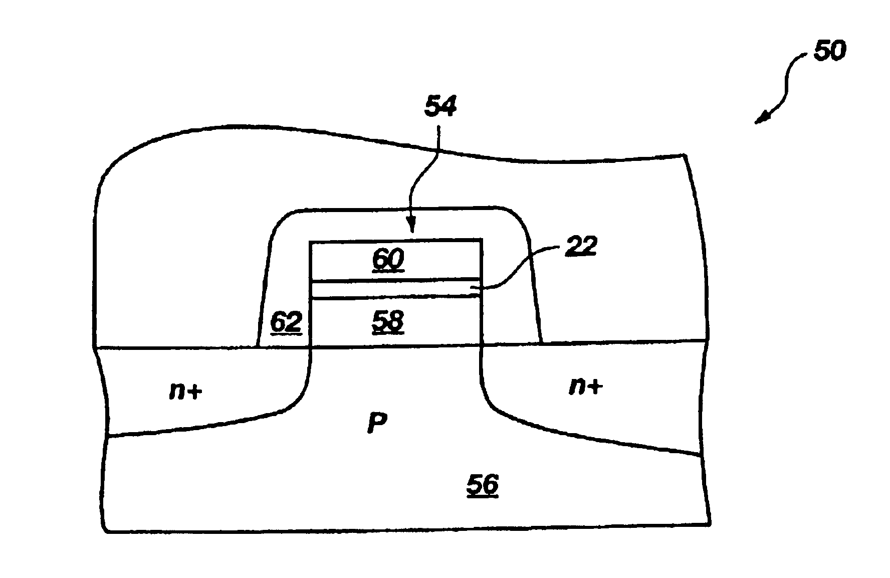
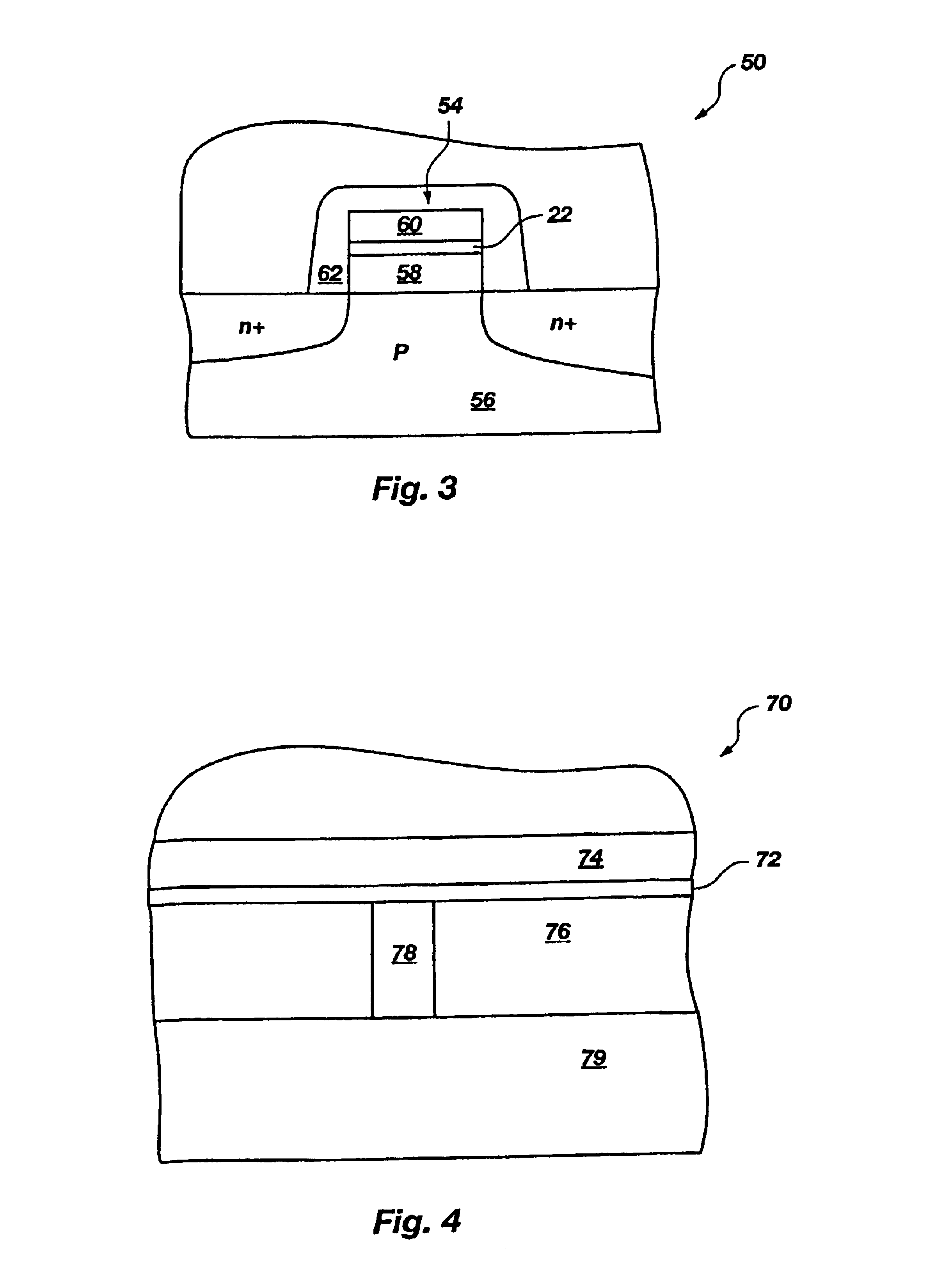
[0022]FIG. 1 shows a partial cross-sectional view of a semiconductor wafer 10 having a tantalum-aluminum-nitrogen (Ta—Al—N) layer 12 between two adjacent layers 14, 16 according to an embodiment of this invention. The Ta—Al—N layer 12 is a conductive alloy formed as a mixture and / or as a compound of tantalum, aluminum and nitrogen. The mixture need not be homogeneous at a microscopic scale. However, an admixture of the elements occurs throughout the Ta—Al—N layer 12.

[0023]The Ta—Al—N layer 12 has desirable properties for serving as a barrier layer, for serving as a wiring line cap layer, for promoting adhesion between adjacent layers, or for defining a contact or electrode. The adjacent layers 14, 16 are formed by any of conductive, non-conductive or semiconductive materials. Typically, the Ta—Al—N layer 12 is between 50 Å and 6000 Å thick. The Ta—Al—N material includes respective atomic concentrations of aluminum, tantalum and nitrogen as follows: between 0.5% and 99.0% aluminum; b...


PUM


Abstract

Ta—Al—N is formed on a semiconductor device structure, such as a wiring line, to prevent interdiffusion between surrounding layers. The Ta—Al—N material may serve as a diffusion between two conductor layers, a semiconductor layer and a conductor layer, an insulator layer and a conductor layer, an insulator layer and a semiconductor layer, or two semiconductor layers. Another use is to promote adhesion of adjacent layers, such as between two conductor layers, a conductor layer and an insulator layer, a semiconductor layer and a conductor layer, or two semiconductor layers. The Ta—Al—N material also may be used to form a contact or electrode.

Description

CROSS-REFERENCE TO RELATED APPLICATIONS[0001]This application is a continuation of U.S. patent application Ser. No. 09 / 207,058, filed Dec. 7, 1998, now U.S. Pat. No. 6,432,818, issued Aug. 13, 2002, which is a divisional of U.S. patent application Ser. No. 08 / 660,849, filed Jun. 10, 1996, now U.S. Pat. No. 5,892,281, issued Apr. 6, 1999.BACKGROUND OF THE INVENTION[0002]This invention relates to materials used in semiconductor device fabrication for interconnects, contacts, electrodes and other conductive applications. More particularly, this invention relates to materials having desirable interdiffusion barrier properties, desirable adhesion properties, and / or low contact resistances.[0003]Semiconductor devices, also called integrated circuits, are mass produced by fabricating hundreds of identical circuit patterns on a single semiconductor wafer. During the process, the wafer is sawed into identical dies or “chips.” Although commonly referred to as semiconductor devices, the device...

Claims


Application Information

Patent Timeline
Patent Type & Authority Patents(United States)
IPC IPC(8): H01L23/52H01L23/532H01L21/768
CPCH01L21/76843H01L21/76849H01L21/7685H01L23/53223H01L2924/12044H01L2924/0002H01L2924/00
Inventor AKRAM, SALMANMEIKLE, SCOTT G.
Owner MICRON TECH INC
Why Eureka
Try Eureka