MRAM field-inducing layer configuration

a field-inducing layer and configuration technology, applied in the field of field-inducing line configurations, can solve problems such as reducing the reliability of devices, and achieve the effects of reducing power requirements, accurate and uniform write selectivity, and improving reliability of devices

Inactive Publication Date: 2005-05-10
CYPRESS SEMICON CORP
View PDF25 Cites 16 Cited by
  • Summary
  • Abstract
  • Description
  • Claims
  • Application Information

AI Technical Summary

Benefits of technology

[0014]There may be several advantages to forming an MRAM device as described herein. In particular, the MRAM device described herein may provide more accurate and uniform write selectivity within an array of magnetic cell junctions arranged within the device. In this manner, the reliability of the device may be increased. In addition, the MRAM device described herein may allow lower currents to be used to switch the magnetic directions of the MRAM cell junctions within the array. Consequently, the MRAM device described herein may function with lower power requirements than conventional MRAM devices.

Problems solved by technology

Such variations of the cell junctions may cause the amount of current needed to switch magnetic cell junctions in the array to vary, thereby reducing the reliability of the device.

Method used


Image

  • MRAM field-inducing layer configuration
  • MRAM field-inducing layer configuration
  • MRAM field-inducing layer configuration

Examples


Embodiment Construction

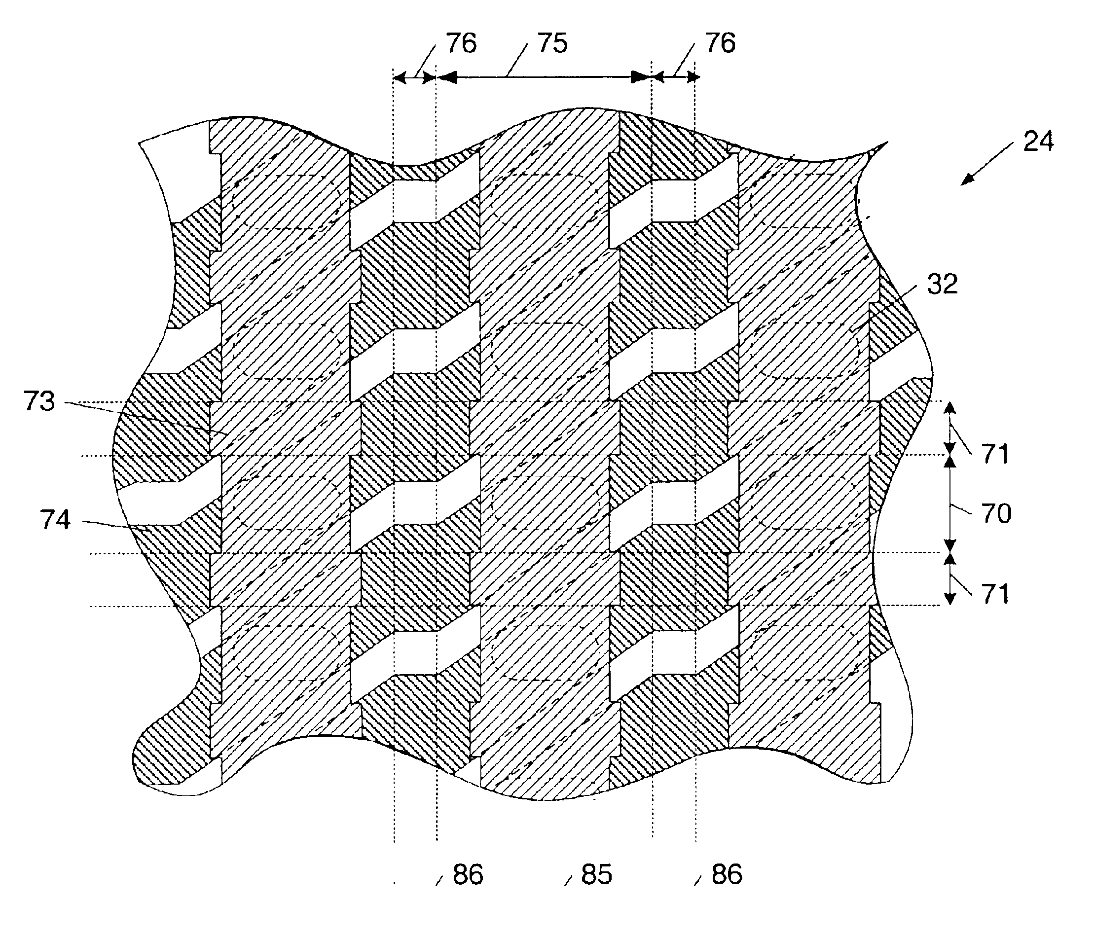
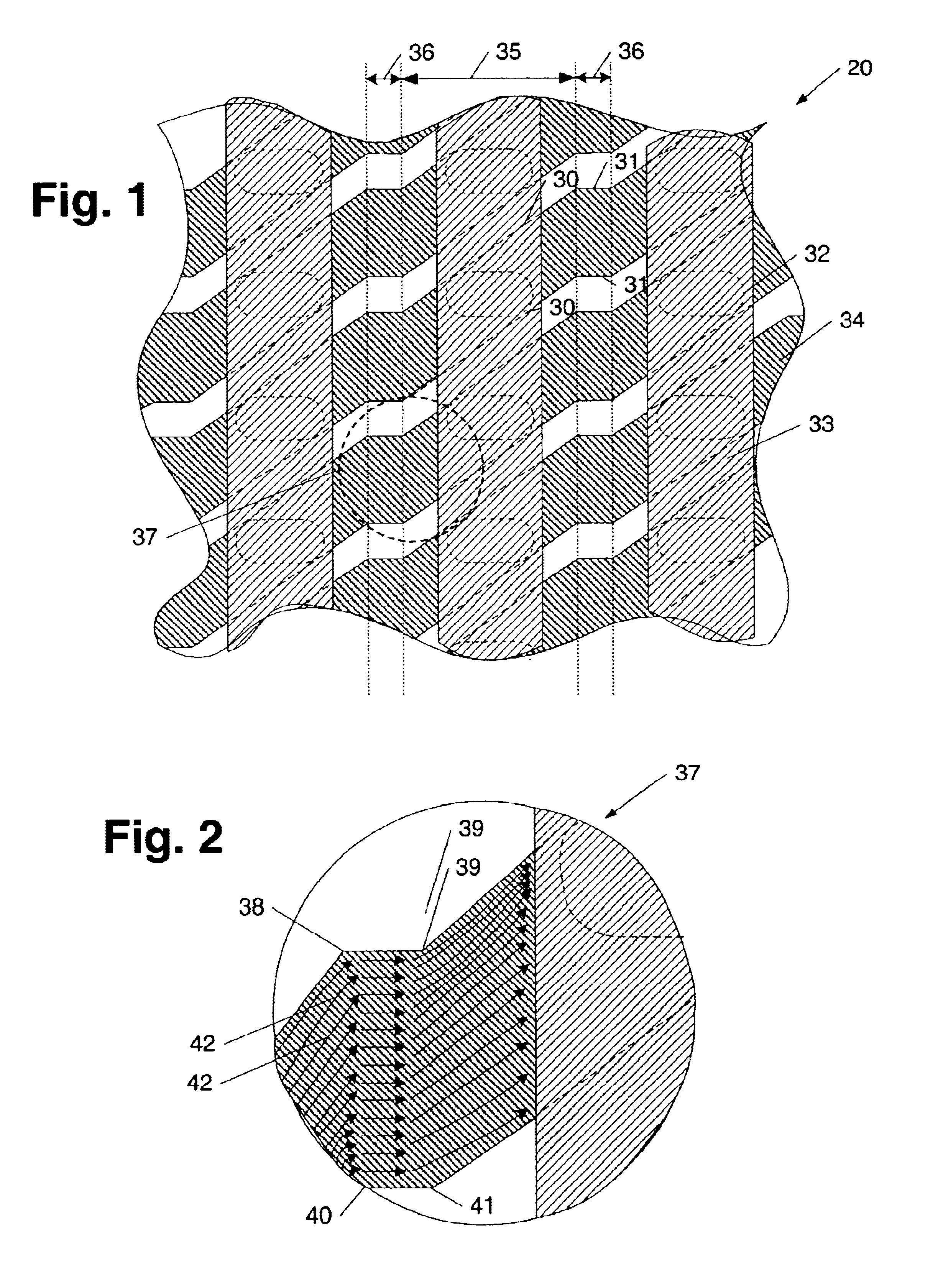
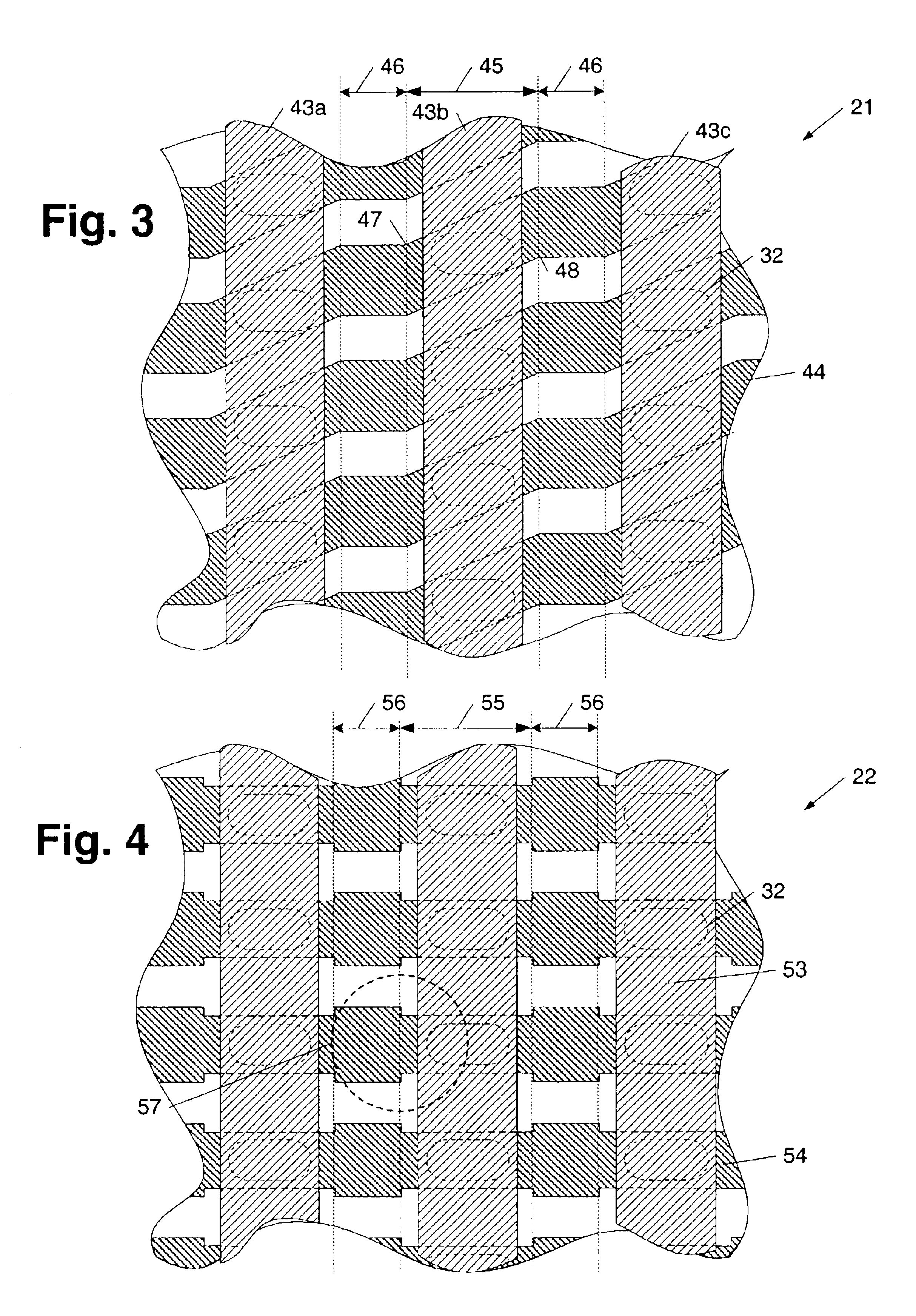
[0029]Turning to the drawings, exemplary embodiments of semiconductor topographies including a conductive line configured to induce a higher magnetic field along at least a portion of a magnetic cell junction included in the semiconductor topography than along a spacing arranged adjacent to the magnetic cell junction are shown in FIGS. 1-10. In particular, FIGS. 1-10 illustrate semiconductor topographies including a plurality of magnetic cell junctions spaced across the topographies and interposed between two sets of field-inducing lines. Each of the field-inducing lines includes first portions aligned with the plurality of the magnetic cell junctions and second portions aligned with spacings arranged between the plurality of magnetic cell junctions. In each embodiment, the first portions of at least one set of the field-inducing lines include a different peripheral profile than second portions of the same field-inducing lines. As explained in more detail below, a field-inducing lin...


PUM


Abstract

A magnetic random access memory (MRAM) device is provided which includes a conductive line configured to induce a magnetic field with a higher magnitude along at least a portion of a magnetic cell junction than along a spacing arranged adjacent to the magnetic cell junction. In some embodiments, the conductive line may include first portions aligned with a plurality of magnetic cell junctions and second portions aligned with spacings arranged between the plurality of magnetic cell junctions. In such an embodiment, the first portions preferably include different peripheral profiles than the second portions. A method for fabricating such an MRAM device is also provided herein. The method may include aligning magnetic cell junctions and first portions of a field-inducing line with each other such that at least part of the first portions of the field-inducing line are configured to conduct a higher density of current than second portions of the field-inducing line.

Description

BACKGROUND OF THE INVENTION[0001]1. Field of the Invention[0002]This invention relates to magnetic memory devices, and more particularly, to field-inducing line configurations arranged adjacent to magnetic cell junctions.[0003]2. Description of the Related Art[0004]The following descriptions and examples are given as background information only.[0005]Recently, advancements in the use of magnetoresistive materials have progressed the development of magnetic random access memory (MRAM) devices to function as viable non-volatile memory circuits. In general, MRAM circuits exploit the electromagnetic properties of magnetoresistive materials to set and maintain information stored within individual magnetic memory cell junctions of the circuit. In particular, MRAM circuits utilize magnetization direction to store information within a memory cell junction, and differential resistance measurements to read information from the memory cell junction. More specifically, information is stored wit...

Claims


Application Information

Patent Timeline
Patent Type & Authority Patents(United States)
IPC IPC(8): H01L27/14H01L27/22
CPCH01L27/222H10B61/00
Inventor SCHWARZ, BENJAMIN C. E.
Owner CYPRESS SEMICON CORP
Why Eureka
Try Eureka