Metal profile for increased local magnetic fields in MRAM devices and method for making the same

Inactive Publication Date: 2007-09-04
MONTEREY RES LLC
View PDF10 Cites 0 Cited by
  • Summary
  • Abstract
  • Description
  • Claims
  • Application Information

AI Technical Summary

Benefits of technology

[0014]There may be several advantages to forming the MRAM device described herein. In particular, the MRAM device described herein may provide more accurate and uniform write selectivity among magnetic cell junctions. In this manner, the reliability of the device may be increased. In addition, the MRAM device described herein may allow lower current to be used to switch the magnetic directions of the MRAM cell junctions within the array. Consequently, the MRAM device described herein may function with lower power requirements than conventional MRAM devices. In addition, the use of lower current may allow smaller on-pitch current drivers to be used, reducing the die size of the MRAM device.

Problems solved by technology

In some cases, the variations of the cell junctions may cause the amount of current needed to switch magnetic cell junctions in the array to vary, thereby reducing the reliability of the device.
Consequently, a reduction in write selectivity reduces the tolerance of the current used to reliably switch selected cells without switching disturbed cells within an array.
In some cases, the tolerance may be too small, allowing a false bit to be unintentionally written to one or more of the disturbed cells and in turn, decrease the functionality of the array.

Method used


Image

  • Metal profile for increased local magnetic fields in MRAM devices and method for making the same
  • Metal profile for increased local magnetic fields in MRAM devices and method for making the same
  • Metal profile for increased local magnetic fields in MRAM devices and method for making the same

Examples


Embodiment Construction

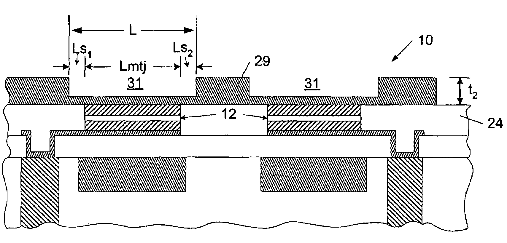
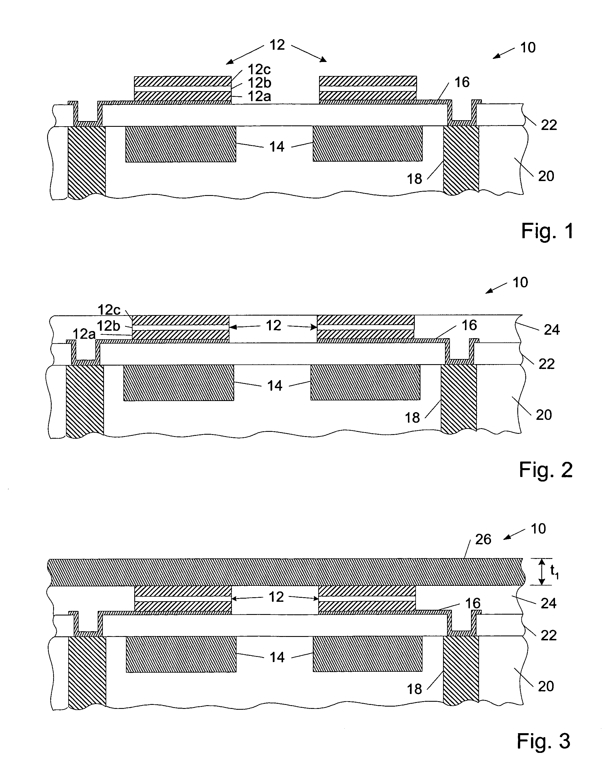
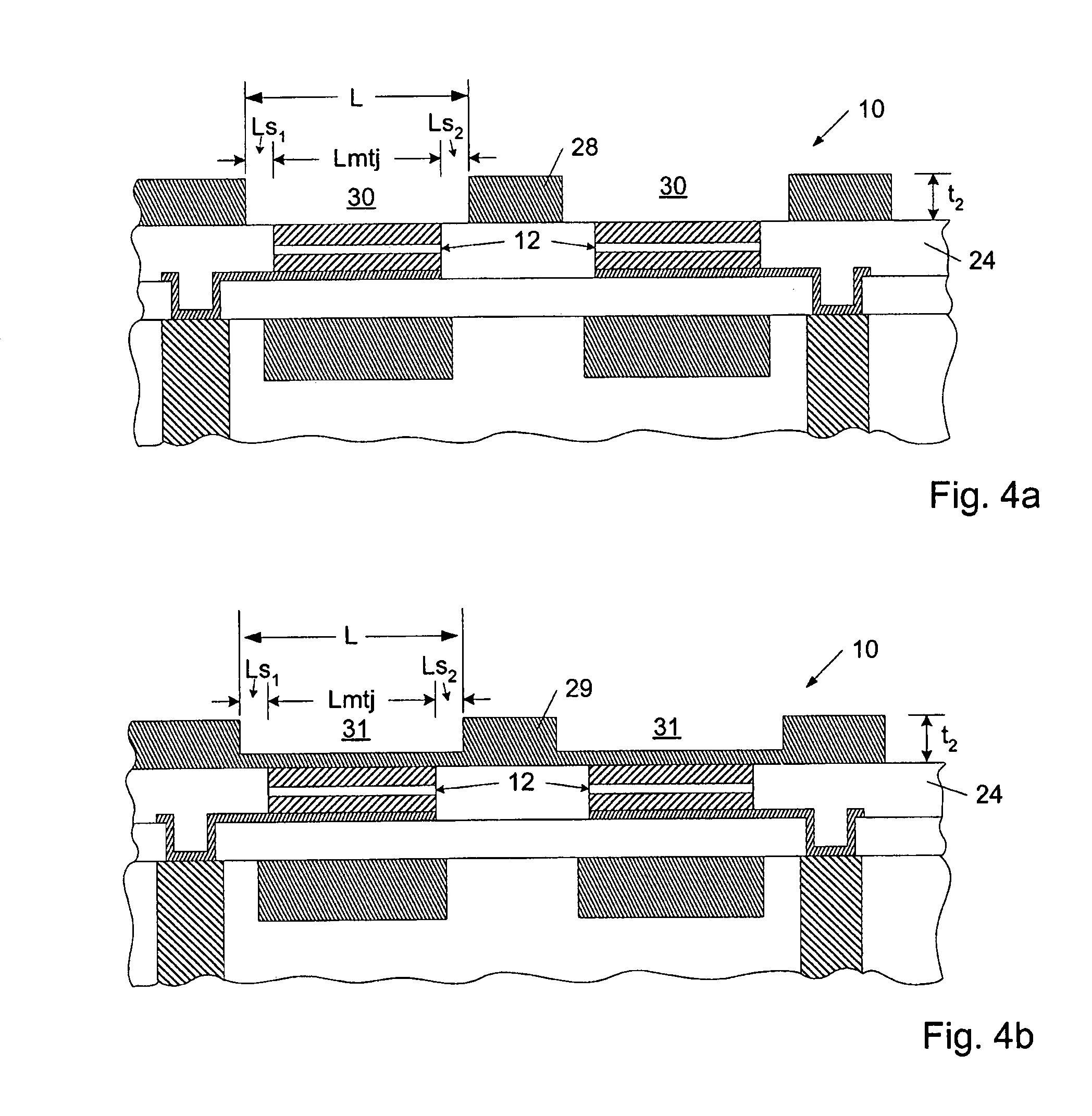
[0025]Turning to the drawings, an exemplary embodiment of a method for fabricating a magnetic random access memory (MRAM) circuit with a conductive line configured to induce a higher magnetic field along at least a portion of a magnetic cell junction than along a spacing arranged adjacent to the magnetic cell junction is shown in FIGS. 1-6. In particular, FIGS. 1-6 depict a method for forming a field-inducing line which is configured to conduct different densities of current therethrough, particularly relative to underlying magnetic cell junctions. Although the method illustrated in FIGS. 1-6 depicts a method for forming a field-inducing line in contact with magnetic cell junctions and, therefore, depicts a method for forming a bit line, the method described herein may alternatively be used to form a digit line spaced above magnetic cell junctions. In addition or alternatively, the devices described herein may include field-inducing lines arranged underneath magnetic cell junctions ...


PUM


Abstract

A method for fabricating a magnetic random access memory circuit (MRAM) and a MRAM circuit resulting therefrom are provided. The method includes depositing a first conductive layer upon and in contact with a plurality of magnetic cell junctions and selectively removing portions of the first conductive layer arranged above the plurality of magnetic cell junctions. In addition, the method includes depositing a second conductive layer above remaining portions of the first conductive layer and the plurality of magnetic cell junctions. The resulting circuit may include a field-inducing line having thickness and / or width variations relative to underlying magnetic cell junctions.

Description

PRIORITY APPLICATION[0001]The present application claims priority to provisional application No. 60 / 505,813 entitled “Metal Profile for Increased Local Magnetic Fields in MRAM Devices and Method for Making the Same,” filed Sep. 25, 2003.BACKGROUND OF THE INVENTION[0002]1. Field of the Invention[0003]This invention relates to magnetic memory devices, and more particularly, to field-inducing line configurations arranged adjacent to magnetic cell junctions.[0004]2. Description of the Related Art[0005]The following descriptions and examples are given as background information only.[0006]Recently, the development of magnetic random access memory (MRAM) devices to function as viable non-volatile memory circuits has been on the forefront of microelectronic technology. In general, MRAM circuits exploit the electromagnetic properties of magnetoresistive materials to set and maintain information stored within individual magnetic memory cell junctions of the circuit. More specifically, MRAM ci...

Claims


Application Information

Patent Timeline
IPC IPC(8): H01L29/76
CPCG11C11/16H01L27/222H01L43/12H10B61/00H10N50/01
Inventor TIEDE, JOHN W.
Owner MONTEREY RES LLC
Why Eureka
Try Eureka