Semiconductor Switch Arrangement and an Electronic Device

Inactive Publication Date: 2008-10-09
NXP USA INC
View PDF7 Cites 15 Cited by
  • Summary
  • Abstract
  • Description
  • Claims
  • Application Information

AI Technical Summary

Benefits of technology

[0015]It is desirable to provide a semiconductor switch arrangement and an elec

Problems solved by technology

As such, a MOSFET device is susceptible to damage when a breakdown voltage is applied to the MOSFET.
However, typically, the breakdown voltage of a zener clamp is relatively low compared to the maximum drain to source voltage of a MOSFET device.
Consequently, this solution can result in a voltage clamp circuit being relative large in size.
Further, the coupling of zener diodes in series can make it difficult to provide an accurate clamp voltage.
Additionally, as the switching characte

Method used


Image

  • Semiconductor Switch Arrangement and an Electronic Device
  • Semiconductor Switch Arrangement and an Electronic Device
  • Semiconductor Switch Arrangement and an Electronic Device

Examples


Embodiment Construction

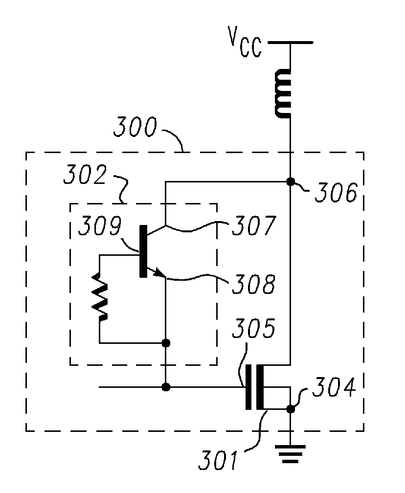
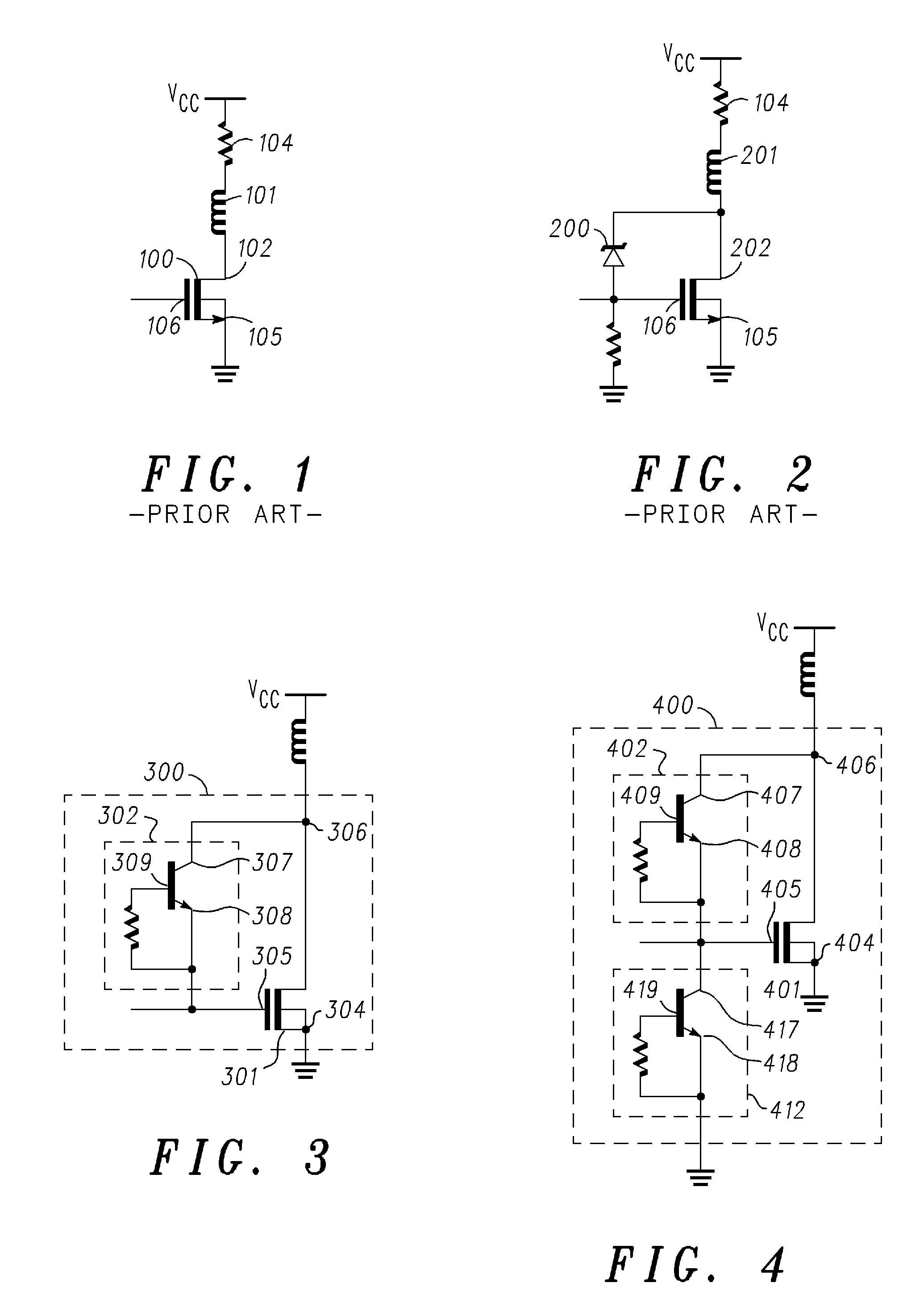
[0029]FIG. 3 shows a semiconductor switch arrangement 300, having a MOSFET device 301 and a bipolar transistor 302, arranged to control the flow of current in an inductive load 303, for example a motor. The source 304 (i.e. input node) of the MOSFET device 301 is electrically coupled to ground, as is a connection to the substrate of the MOSFET device 301. The gate 305 (i.e. control node) of the MOSFET device 301 is electrically coupled to a control circuit (not shown) for controlling the switching of the MOSFET device 301. The drain 306 of the MOSFET device 301 is coupled to a supply voltage Vcc, via the inductive load 303.

[0030]Although the preferred embodiment of the present invention uses a MOSFET device to provide the switching facility, other forms of semiconductor switches could be used, for example, IGBT, GTO, and power bipolar transistors.

[0031]The MOSFET device 301 illustrated is an N-type device. However, as would be appreciated by a person skilled in the art, a P-type dev...


PUM


Abstract

A semiconductor switch arrangement ( 300 ) comprises a bipolar transistor ( 302 ) and a semiconductor power switch ( 301 ) having an input node ( 306 ), an output node ( 304 ) and a control node ( 305 ) for allowing a current path to be formed between the input node ( 306 ) and the output node ( 307 ). The bipolar transistor ( 302 ) is coupled between the input node ( 306 ) and the control node ( 305 ) such that upon receiving an electro-static discharge pulse the bipolar transistor ( 302 ) allows a current to flow from the input node ( 306 ) to the control node ( 305 ) upon a pre-determined voltage being exceeded at the input node ( 306 ) to allow the control node ( 305 ) to cause a current to flow from the input node ( 306 ) to the output node ( 307 ). Thus, the bipolar transistor device protects the semiconductor switch device, such as an LDMOS device, against ESD, namely protection against power surges of, say, several amperes in less than 1 usec.

Description

FIELD OF THE INVENTION[0001]The present invention relates to a semiconductor switch arrangement for an electronic device.BACKGROUND OF THE INVENTION[0002]Semiconductor power switches, for example MOSFET devices, are frequently used to control the flow of current within an electronic device, and in particular to control the supply of current through an inductive load, such as those used in large motors and generators.[0003]By way of illustration a MOSFET device 100 configured to operate as a switch for controlling a current through an inductive load 101 is shown in FIG. 1, where the drain 102 of a MOSFET device 100 is coupled to a voltage supply Vcc via the inductive load 101 and a resistive load 104, the source 105 of the MOSFET device 100 is coupled to ground and the gate 106 of the MOSFET device 100 is coupled to a control signal for switching the MOSFET device on or off (i.e. cause the drain / source to become closed or open circuit).[0004]For an N-channel MOSFET device a positive ...

Claims


Application Information

Patent Timeline
IPC IPC(8): H03K17/082
CPCH03K17/0822
Inventor ZECRI, MICHELBERTOLINI, LUCABESSE, PATRICEBAFLEUR, MARYSENOLHIER, NICOLAS
Owner NXP USA INC
Why Eureka
Try Eureka