Radiation-emitting semiconductor chip and light-emitting diode

Inactive Publication Date: 2005-05-10
OSRAM OLED
View PDF37 Cites 20 Cited by
  • Summary
  • Abstract
  • Description
  • Claims
  • Application Information

AI Technical Summary

Benefits of technology

[0005]Proceeding from this state of the art, an object of the invention is to provide a semiconductor chip suitable for high radiation efficiencies and offering improv

Problems solved by technology

The light output is limited substantially by absorption in the semiconductor chip.
Problems arise with the known semiconductor

Method used


Image

  • Radiation-emitting semiconductor chip and light-emitting diode
  • Radiation-emitting semiconductor chip and light-emitting diode
  • Radiation-emitting semiconductor chip and light-emitting diode

Examples


example 2

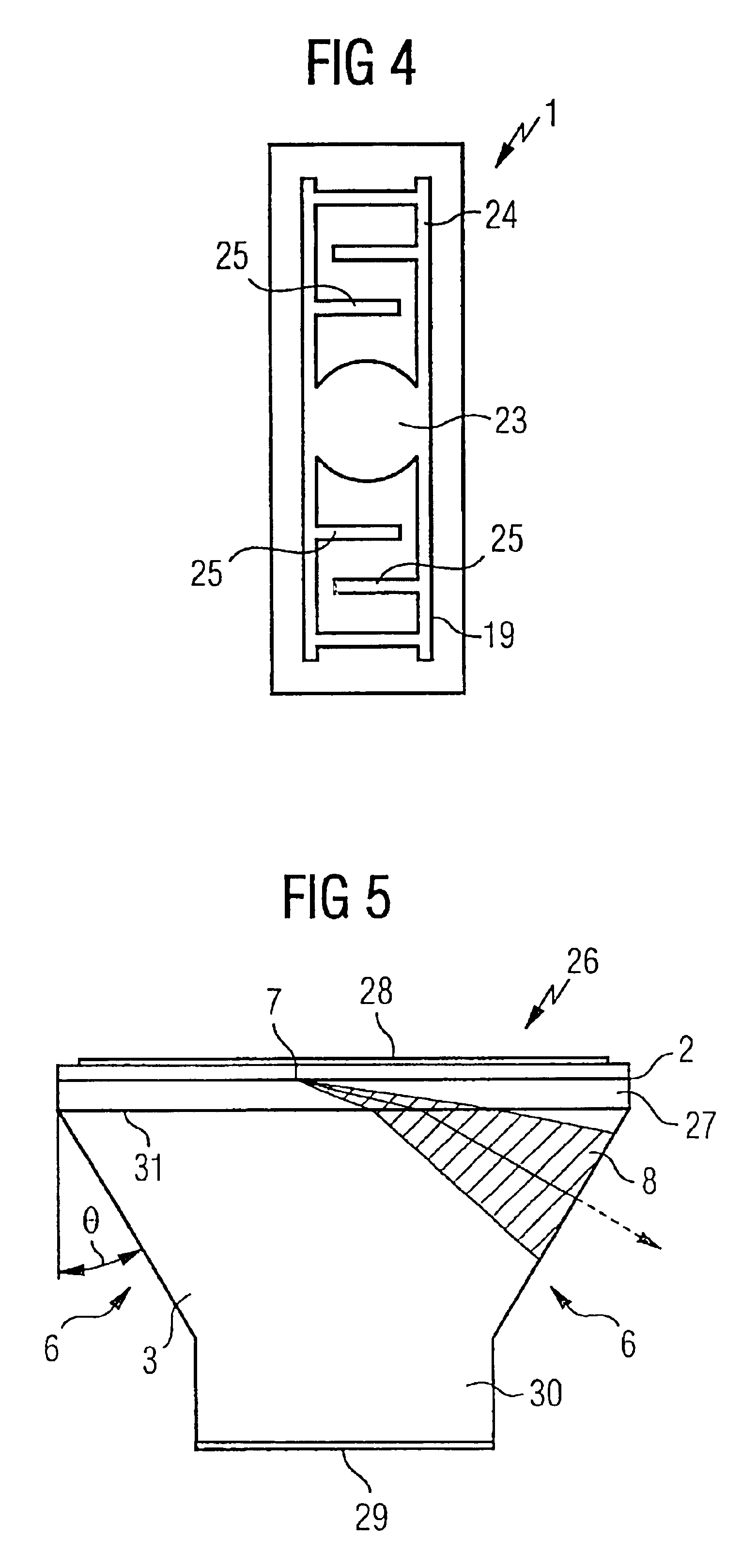
[0045]In the case of the semiconductor chip 26 with inclined sides illustrated in FIG. 5, the following values, presented in Table 2, were found for the various types. The percentage of extracted radiation has been referred to the total extraction obtained with the standard chip, as stated in Table 1.

[0046]

TABLE 2Cross-SectionalLateralTypeArea × HeightCurrentFrontsurfacesTotalStandard chip = 250 × 50 mA50%150%200%reference250 μm2 ×250 μmLarge chip750 ×450 mA450%400%850%750 μm2 ×250 μmRectangular chip250 ×450 mA450%1100%1550%2250 μm2 ×250 μm

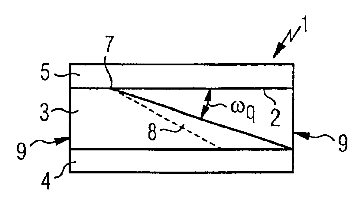
[0047]Compared to the large chip of equal area, semiconductor chip 26 of FIG. 5 shows an improvement factor of 1.8, while in the case of semiconductor chip 1 of FIGS. 1a and 1b the gain is roughly 15%. Thus, lengthening the longitudinal sides 6 relative to the transverse sides 9 produces a marked increase in light output.

[0048]It should be noted that the considerations presented herein also apply to a semiconductor chip in which the active layer h...


PUM


Abstract

Proposed for high-performance light-emitting diodes are semiconductor chips (1) whose longitudinal sides are substantially longer than their transverse sides. Light extraction can be substantially improved in this manner.

Description

FIELD OF THE INVENTION[0001]The invention concerns a radiation-emitting semiconductor chip comprising an active layer that includes a radiation-producing region, and comprising transverse sides and longitudinal sides that delimit the semiconductor laterally in a direction of extent of the active region. The invention further concerns a light-emitting diode (LED) fashioned with such a semiconductor chip.BACKGROUND OF THE INVENTION[0002]A semiconductor chip of this kind is known from the article by Song Jae Lee and Seok Won Song, “Efficiency Improvement in Light-Emitting Diodes Based on Geometrically Deformed Chips,” SPIE Conference on Light-Emitting Diodes: Research, Manufacturing and Applications III, San Jose, Calif., January 1999, pages 237-248. The semiconductor body of a semiconductor chip described therein comprises a bottom cover layer, an active region and a top cover layer. In one embodiment, the semiconductor chip is realized in the shape of a prism with a lozenge as its ba...

Claims


Application Information

Patent Timeline
IPC IPC(8): H01L33/00H01L33/20H01L33/24
CPCH01L33/20H01L33/24H01L2224/48091H01L2924/00014
Inventor BAUR, JOHANNESEISERT, DOMINIKFEHRER, MICHAELHAHN, BERTHOLDHARLE, VOLKERJACOB, ULRICHPLASS, WERNERSTRAUSS, UWEVOLKL, JOHANNESZEHNDER, ULRICH
Owner OSRAM OLED
Why Eureka
Try Eureka