Light emitting device

a light-emitting device and light-emitting technology, which is applied in the direction of semiconductor devices, basic electric elements, electrical equipment, etc., can solve the problems of low excitation efficiency of light-emitting devices and the inability to convert at high efficiency the wavelength of light from the light-emitting element to radiate outside, etc., to achieve high luminance, high efficiency, and high luminance

Inactive Publication Date: 2005-05-10
TOYODA GOSEI CO LTD
View PDF12 Cites 110 Cited by
  • Summary
  • Abstract
  • Description
  • Claims
  • Application Information

AI Technical Summary

Benefits of technology

[0007]In the above light emitting device, the fluorescent material is excited by the light in the ultraviolet region emitted by the light-emitting element and emits light. And the light by such emission and the light in the visible region emitted by the light-emitting element are mixed and radiated outside. Herein, since the light in the ultraviolet region emitted by the light-emitting element is utilized for exciting the fluorescent material, the fluorescent material can be excited at high efficiency and emission at high luminance can be obtained from the fluorescent material. On the other hand, the light in the visible region is emitted from the light-emitting element, and this light is not absorbed by the fluorescent material but radiated outside. Accordingly, the light in the visible region emitted by the light-emitting element can be utilized as externally radiating light without loss.
[0008]As mentioned above, by adopting a structure of using the light-emitting element emitting light in the ultraviolet region and light in the visible region and utilizing the light in the ultraviolet region for exciting the fluorescent material, the emission of high luminance can be obtained from the fluorescent material, and at the same time, the light of the light-emitting element can be suppressed from loss. That is, a light emitting device is provided, which utilizes the light of the light-emitting element at high efficiency and has high emission efficiency.

Problems solved by technology

Accordingly, the above light emitting device is low in the excitation efficiency of the fluorescent material, and it cannot convert at high efficiency the wavelength of the light from the light-emitting element to radiate it outside.

Method used


Image

  • Light emitting device
  • Light emitting device
  • Light emitting device

Examples


Embodiment Construction

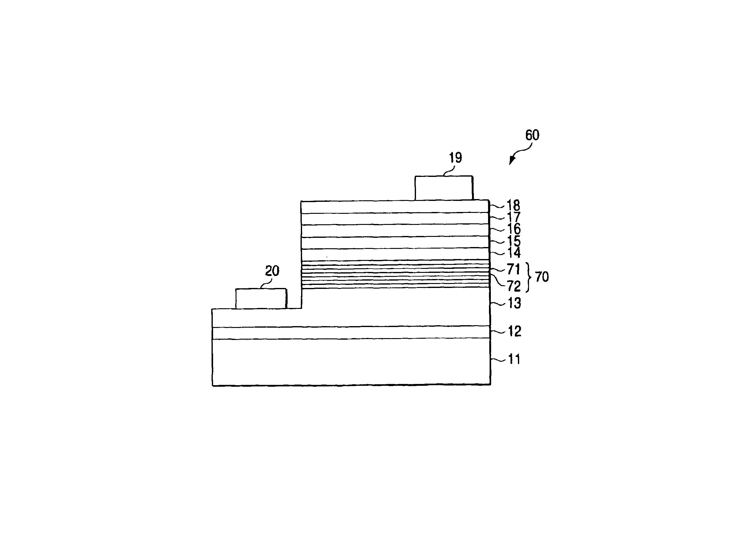
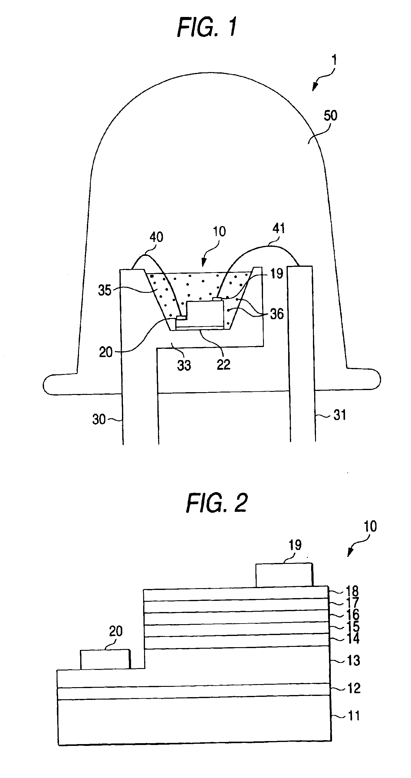
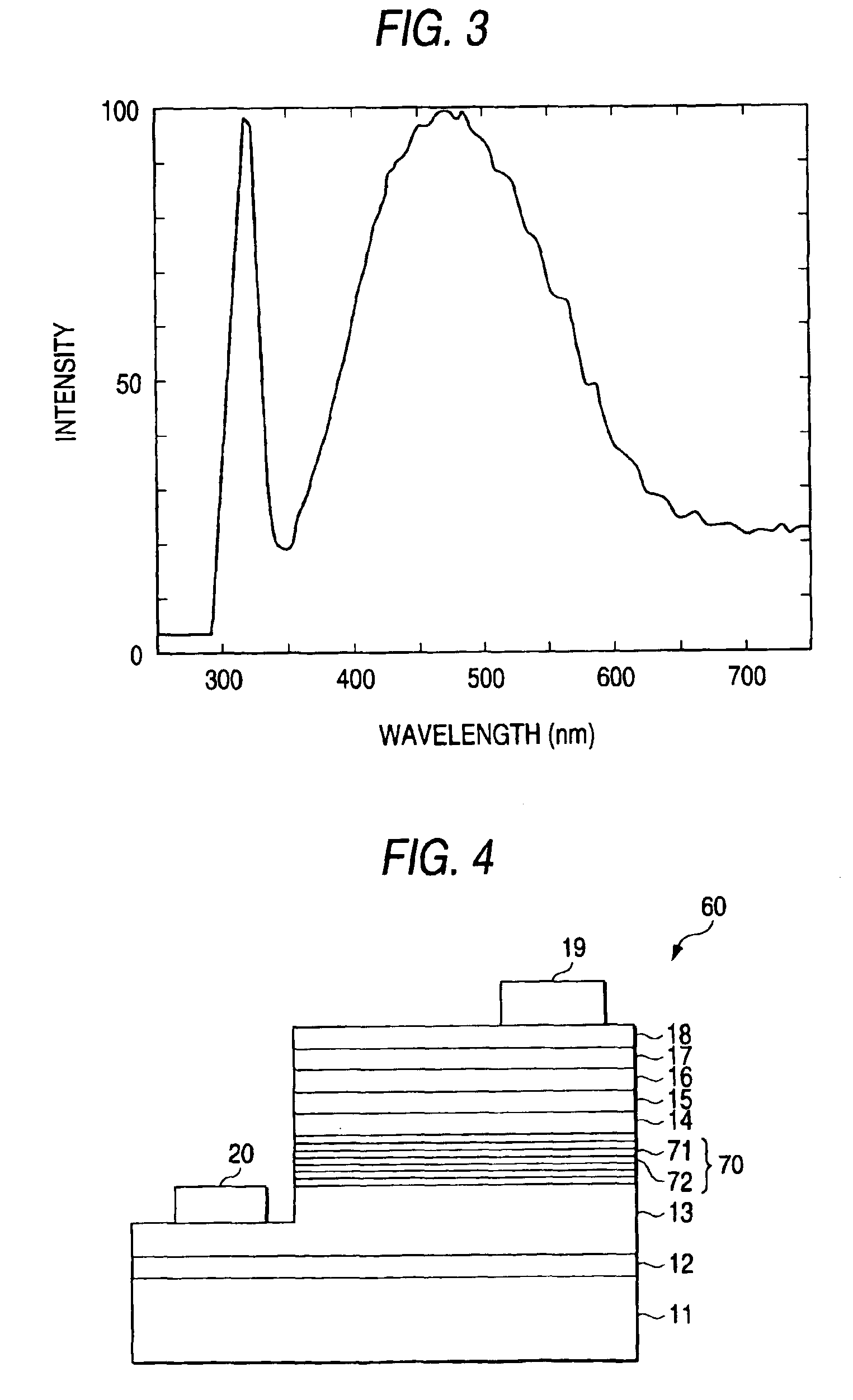
[0013]The light-emitting element of the invention has a light-emitting layer comprising the Group III nitride compound semiconductor, and emitting light with an emission peak wavelength in the ultraviolet region and light with an emission peak wavelength in the visible region. That is, as to the emission wavelength, the light-emitting element uses the light-emitting layer having respectively at least one emission peak in the ultraviolet region and at least one emission peak in the visible region. As far as the light-emitting layer satisfies this condition, it is possible to use the light-emitting layer having two or more emission peaks in the ultraviolet region, and to use the light-emitting layer having two or more emission peaks in the visible region.

[0014]The light in the ultraviolet region must be able to excite a fluorescent material described hereinafter, preferably the light has the wavelength which can excite the fluorescent material at high efficiency. Accordingly, the ligh...


PUM


Abstract

According to the invention, a Group III nitride compound semiconductor light-emitting element is provided with a light-emitting layer comprising two layers of different in ratio of AlGaInN composition, and emitting light with an emission peak wavelength in an ultraviolet region and light with an emission peak wavelength in a visible region. The light-emitting element and a fluorescent material excited by light in the ultraviolet region are combined to configure a light emitting device.

Description

TECHNICAL FIELD[0001]The present invention relates to a light emitting device. In particular, the present invention relates to a light emitting device which is made by a combination of a Group III nitride compound semiconductor light-emitting element and a fluorescent material, and converts a part of light emitted from the light-emitting element by the fluorescent material to thereby emit light.BACKGROUND ART[0002]There has been proposed a light emitting device which changes wavelength of a part of light from the light-emitting element by the fluorescent material, and mixes the light which has been subjected to wavelength conversion and the light from the light-emitting element, thereby enabling to emit a color different from an emission light color of the light-emitting element itself. For example, a light emitting device which has a structure where a light-emitting element for emitting blue light and a fluorescent material excited by the blue light to thereby emit light with wavel...

Claims


Application Information

Patent Timeline
Patent Type & Authority Patents(United States)
IPC IPC(8): H01L33/00H01L27/15H01L33/10H01L33/32H01L33/50H01L33/52H01L33/62
CPCH01L33/08H01L33/32H01L33/50H01L2224/73265H01L2924/01025H01L2924/01079H01L2924/12041H01L2224/49107
Inventor KOZAWA, TAKAHIROSHIBATA, NAOKI
Owner TOYODA GOSEI CO LTD
Why Eureka
Try Eureka