Measuring method, inspection method, inspection device, semiconductor device, method of manufacturing a semiconductor device, and method of manufacturing an element substrate

a technology of inspection method and inspection method, which is applied in the direction of individual semiconductor device testing, semiconductor/solid-state device testing/measurement, instruments, etc., can solve the problems of increasing the time required to perform the whole manufacturing process, complicated inspection steps, and difficulty in determining whether a circuit or a circuit element is defective or non-defectiv

Inactive Publication Date: 2005-05-10
SEMICON ENERGY LAB CO LTD
View PDF11 Cites 69 Cited by
  • Summary
  • Abstract
  • Description
  • Claims
  • Application Information

AI Technical Summary

Benefits of technology

[0014]The present invention has been made in view of the above-described problems, and an object of the present invention is to establish a further simpli

Problems solved by technology

The optical inspection method have a problem in that if the inspection is performed after the completion of formation of a plurality of layered patterns, it is difficult to identify each pattern in lower layers, and it is, therefore, difficult to determine whether a circuit or a circuit element is defective or non-defective by performing detection of a defective portion.
In such a case, however, the inspection step is c

Method used


Image

  • Measuring method, inspection method, inspection device, semiconductor device, method of manufacturing a semiconductor device, and method of manufacturing an element substrate
  • Measuring method, inspection method, inspection device, semiconductor device, method of manufacturing a semiconductor device, and method of manufacturing an element substrate
  • Measuring method, inspection method, inspection device, semiconductor device, method of manufacturing a semiconductor device, and method of manufacturing an element substrate

Examples


embodiment 1

(Embodiment 1)

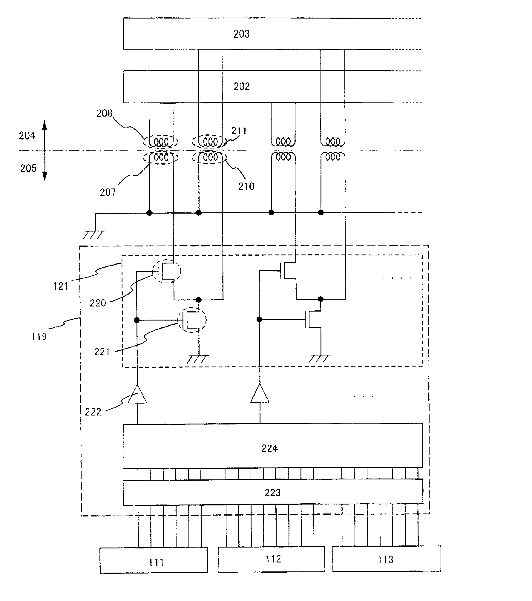
[0303]Embodiment 1 of the present invention will be described with respect to an example of inspection performed in such a manner that while no output primary coils and no output secondary coils are provided, weak electromagnetic waves or electric fields generated when circuits of the circuit elements are driven are monitored to detect a portion not operating normally in a multiplicity of the circuits or circuit elements.

[0304]FIG. 10 shows the structures of an element substrate 455 and an inspection substrate 454 in this embodiment. The element substrate 455 has an inspection-only circuit 419. The inspection-only circuit 419 has means for performing signal processing on outputs from the circuits of the circuit elements, which are objects to be inspected, to form signals (operation information signals) including information on the operating conditions of the inspected circuits or circuit elements. In this embodiment, an A / D converter circuit 473 and a data format secti...

embodiment 2

(Embodiment 2)

[0327]Inspection drive signals and power supply voltages in a liquid crystal display and an OLED display will be described in more detail as an example.

[0328]The number of primary and secondary coils is changed according to the constructions of the pixel portion and the drive circuits on the element substrate. Therefore it is important to set the number of coils according to the specifications of each element substrate.

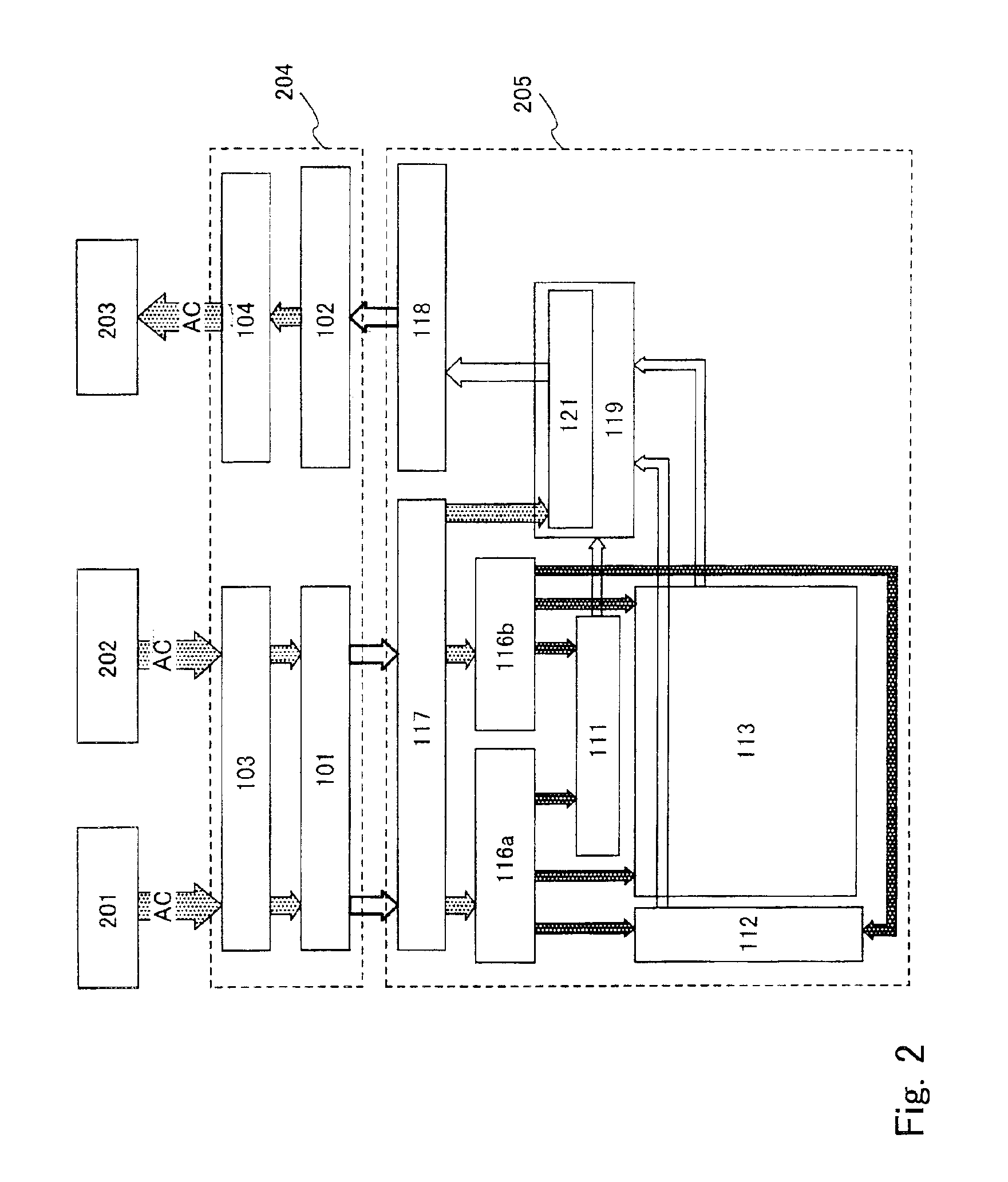
[0329]FIG. 11 shows the structure of circuits on an element substrate of an ordinary liquid crystal display. The element substrate shown in FIG. 11 has a signal line drive circuit 700, a scanning line drive circuit 701, and a pixel portion 702.

[0330]A plurality of signal lines and a plurality of scanning lines are formed in the pixel portion 702. A region between signal lines and between scanning lines corresponds to a pixel forming segment. Only a pixel forming segment with one signal line 703 and one scanning line 704, which is representative of a plur...

embodiment 3

(Embodiment 3)

[0363]An embodiment of the present invention will be described which relates to cutting of a large-size element substrate from which a plurality of display substrates are formed after inspection.

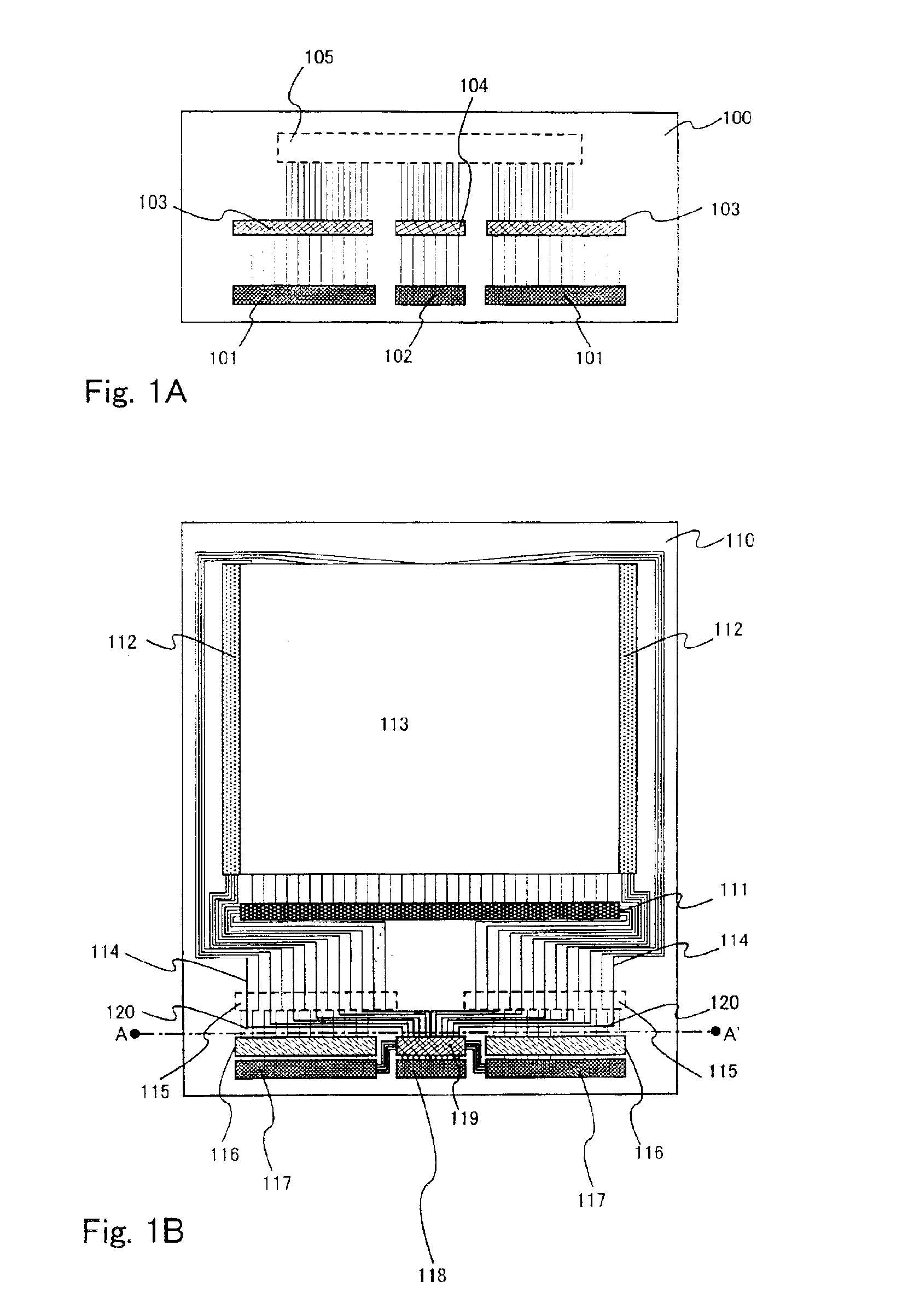
[0364]FIG. 13 is a top view of a large-size element substrate (also called an array substrate) before the substrate is cut. A pixel portion 1001, a scanning line drive circuit 1002, and a signal line drive circuit 1003 are provided on the element substrate. In the region indicated by 1004, there are formed circuits or circuit elements, such as a plurality of input secondary coils, a plurality of output primary coils, a waveform shaping circuit, a rectifier circuit, and an inspection-only circuit, which are used only in an inspection step, and which are not used after the completion of the inspection step.

[0365]The element substrate is cut along a line represented by a dotted line in FIG. 13, thus forming nine display substrates from one element substrate. While this embodiment ...


PUM


Abstract

An inspection method which simplifies an inspection step by eliminating the need to set probes on wiring or probe terminals, and an inspection device for performing the inspection step. A voltage is applied to each of inspected circuits or circuit elements to operate the same. Signal processing is performed on an output from each inspected circuit or circuit element during operation to form a signal (operation information signal) including information on the operating condition of the circuit or the circuit element. The operation information signal is amplified and the amplitude of an alternating current voltage separately input is modulated with the amplified operation information signal. The voltage of the modulated alternating current is read in a non-contact manner to determine whether the corresponding circuit or circuit element is non-defective or defective.

Description

BACKGROUND OF THE INVENTION[0001]1. Field of the Invention[0002]The present invention relates to a measuring method in which a circuit or a circuit element of a semiconductor device is operated and an output from the circuit or the circuit element is read, and to a method of inspecting by using the measuring method to inspect whether a pixel portion operates normally. More particularly, the present invention relates to a non-contact type inspection method and a non-contact type inspection device using the non-contact type inspection method. The present invention also relates to a method of manufacturing a semiconductor device, which includes an inspection step using the inspection method, and to a semiconductor device manufactured by using the manufacturing method. Further, the present invention relates to a method of manufacturing an element substrate including an inspection step using the inspection method, and to an element substrate manufactured by using the manufacturing method...

Claims


Application Information

Patent Timeline
IPC IPC(8): G01R31/01G01R1/06G01R31/265G01R31/302G02F1/13G02F1/1368H01L21/66
CPCG01R31/01G01R31/265G01R31/26H01L22/00G01R1/07G01R19/0084
Inventor HIROKI, MASAAKI
Owner SEMICON ENERGY LAB CO LTD
Why Eureka
Try Eureka