Method of fabricating a flash memory

a technology of flash memory and floating gate, which is applied in the direction of basic electric elements, semiconductor devices, electrical apparatus, etc., can solve the problems of difficult to improve the performance of the memory device, very little power consumption, etc., and achieve the effect of improving device performance and enhancing the gate coupling ratio

Active Publication Date: 2005-05-17
POWERCHIP SEMICON MFG CORP
View PDF2 Cites 18 Cited by
  • Summary
  • Abstract
  • Description
  • Claims
  • Application Information

AI Technical Summary

Benefits of technology

[0013]Accordingly, the present invention is directed to a method of fabricating a flash memory adapted to enhance the gate coupling ratio between the floating gate and the control gate for improving device performance.

Problems solved by technology

In addition, the flash memory is also a type of high-speed non-volatile memory (NVM) that occupies very little space and consumes very little power.
In the absence of any other method for increasing the overlapping area between the control gate and the floating gate, improving the performance of the memory device is difficult.

Method used


Image

  • Method of fabricating a flash memory
  • Method of fabricating a flash memory
  • Method of fabricating a flash memory

Examples


Embodiment Construction

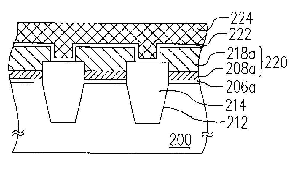
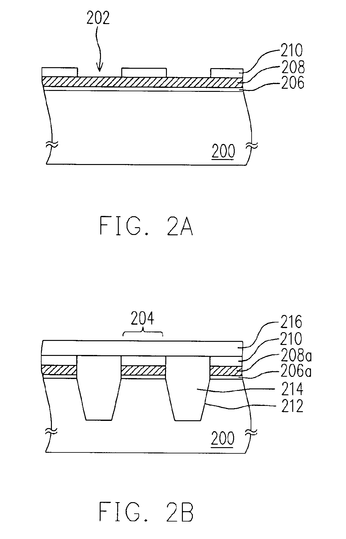
[0024]Reference will now be made in detail to the present preferred embodiments of the invention, examples of which are illustrated in the accompanying drawings. Wherever possible, the same reference numbers are used in the drawings and the description to refer to the same or like parts.

[0025]FIGS. 2A through 2E are schematic cross-sectional views showing the steps for fabricating a flash memory according to one embodiment of the present invention.

[0026]As shown in FIG. 2A, a substrate 200 such as a silicon substrate is provided. Thereafter, a tunneling dielectric layer 206, a conductive layer 208 and a patterned mask layer 210 are sequentially formed over the substrate 200. The patterned mask layer 210 has openings 202 that expose areas for forming a device isolation structure.

[0027]The tunneling dielectric layer 206 is silicon oxide layer having a thickness between about 70 Å to 90 Å formed, for example, by performing a thermal oxidation process. The conductive layer 208 is a dope...


PUM


Abstract

A method of fabricating a flash memory is provided. A substrate having several device isolation structures for defining an active region is provided. A tunneling dielectric layer and a patterned mask layer are sequentially formed over the active region of the substrate. A sacrificial layer is formed on the substrates. Thereafter, the sacrificial layer is patterned to retain a part of sacrificial layer on the device isolation structures. The patterned mask layer is removed, and a conductive layer that exposed the top section of the sacrificial layers is formed over the substrate. After removing the sacrificial layer, an inter-gate dielectric layer is formed over the substrate. A control gate is formed over the inter-gate dielectric layer. Finally, a source region and a drain region are formed in the substrate on each side of the control gate.

Description

CROSS REFERENCE TO RELATED APPLICATIONS[0001]This application claims the priority benefit of Taiwan application serial no. 93103279, filed Feb. 12, 2004.BACKGROUND OF INVENTION[0002]1. Field of the Invention[0003]The present invention relates to a method of fabricating a memory device. More particularly, the present invention relates to a method of fabricating a flash memory and floating gate.[0004]2. Description of Related Art[0005]Flash memory is a type of electrically erasable programmable read-only memory (EEPROM). Flash memory is a memory device that allows multiple data writing, reading and erasing operations. The stored data will be retained even after power to the device is removed. With these advantages, it has been broadly applied in personal computer and electronic equipment. In addition, the flash memory is also a type of high-speed non-volatile memory (NVM) that occupies very little space and consumes very little power. Moreover, erasing is carried out in a block-by-blo...

Claims


Application Information

Patent Timeline
Patent Type & Authority Patents(United States)
IPC IPC(8): H01L21/02H01L21/336H01L21/8247H01L27/115
CPCH01L27/11521H01L27/115H10B69/00H10B41/30
Inventor WANG, LEODU, CHIEN-CHIHPITTIKOUN, SAYSAMONE
Owner POWERCHIP SEMICON MFG CORP
Why Eureka
Try Eureka