Monolithic nonlinear transmission lines and sampling circuits with reduced shock-wave-to-surface-wave coupling

a nonlinear transmission line and coupling technology, applied in waveguides, line-transmission details, instruments, etc., can solve the problems of short fall times of shock waves, inability to reduce reduced shock wave to surface wave coupling, so as to reduce the coupling between shock waves and reduce the coupling. , the effect of reducing the coupling

Inactive Publication Date: 2005-05-17
ANRITSU CO
View PDF10 Cites 20 Cited by
  • Summary
  • Abstract
  • Description
  • Claims
  • Application Information

AI Technical Summary

Benefits of technology

[0007]A monolithic non-linear transmission line and sampling circuit with reduced shock-wave-to-surface-wave coupling are presented herein. In coplanar-waveguide (CPW) technology, this reduced coupling is achieved by selecting properly the thickness of the semiconductor substrate, and by elevating the center conductor of the CPW above the substrate surface. The elevated center conductor is supported by means of conducting posts, and may be backed by a low-loss dielectric such as polyimide or silicon nitride. In coplanar-strip (CPS)...

Problems solved by technology

Although nonlinear transmission lines having a top-contacted air-bridged center conductor have been developed, their ability to reduce shock-wave-to-surface-wave coupling has not been recognized.
In operation, these nonlinear transmission lines reduce high skin-effect losses at extremely short wavelengths, and result in shock waves having short fall times. The reduced shock-wave-to-surface-wave coupling resulting from the elevation of the center conductor above the substrate surface has not been recognized, nor...

Method used


Image

  • Monolithic nonlinear transmission lines and sampling circuits with reduced shock-wave-to-surface-wave coupling
  • Monolithic nonlinear transmission lines and sampling circuits with reduced shock-wave-to-surface-wave coupling
  • Monolithic nonlinear transmission lines and sampling circuits with reduced shock-wave-to-surface-wave coupling

Examples


Embodiment Construction

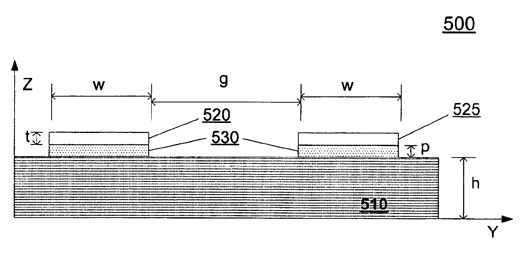
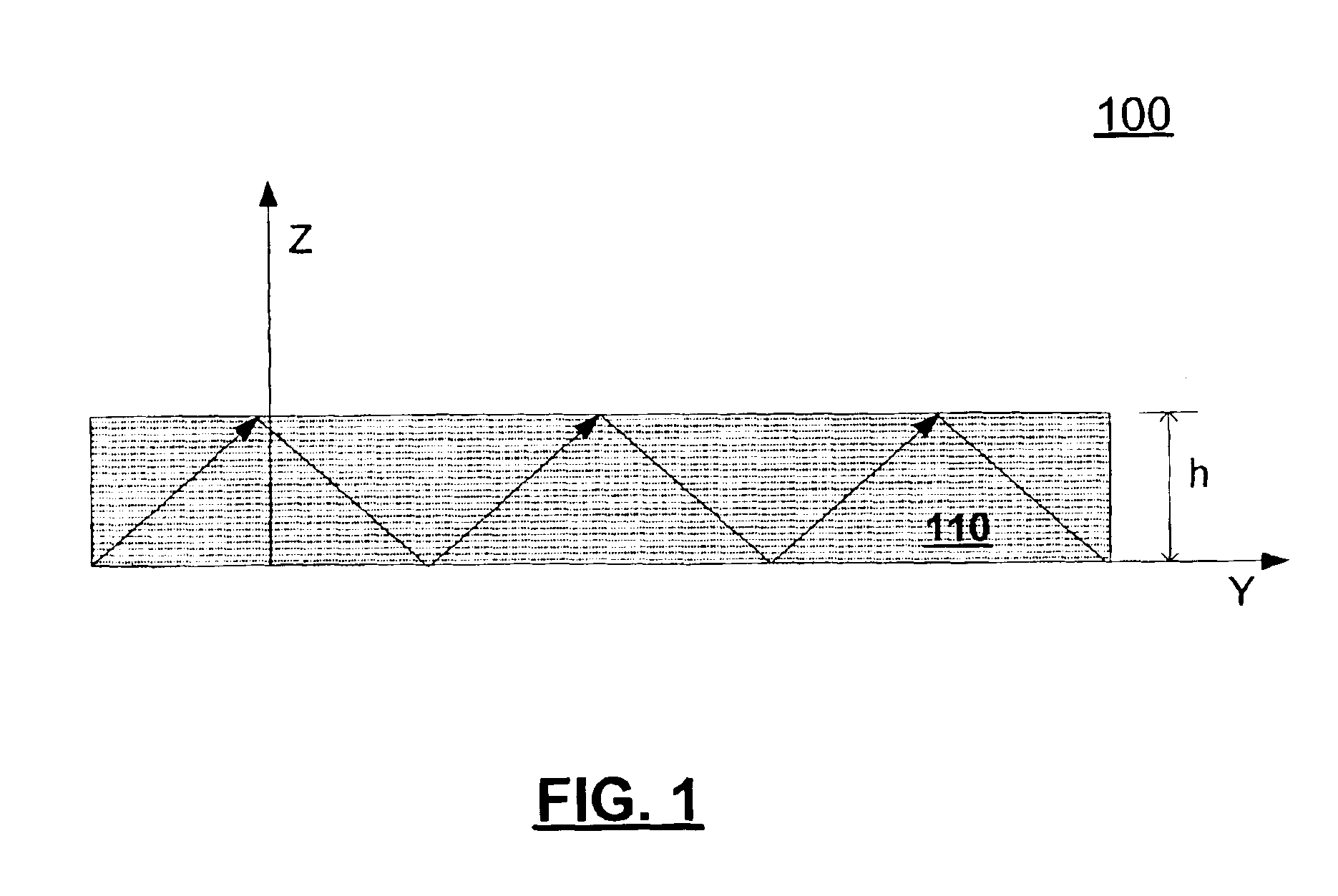
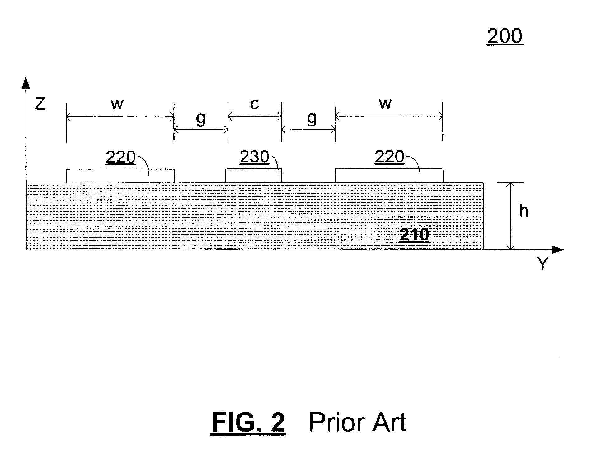
[0014]A monolithic non-linear transmission line and sampling circuit with reduced shock-wave-to-surface-wave coupling are presented herein. In coplanar-waveguide (CPW) technology, this reduced coupling is achieved by selecting properly the thickness of the semiconductor substrate, and by elevating the center conductor of the CPW above the substrate surface. The elevated center conductor is supported by means of conducting posts, and may be backed by a low-loss dielectric such as polyimide or silicon nitride. In coplanar-strip (CPS) technology, the reduction in coupling between shock waves and surface waves is achieved by controlling the substrate thickness as in the CPW case, and by elevating the coplanar strips above the substrate surface. The elevated strips are supported by a low-loss dielectric. The reduced coupling in both guiding media enhances the high-frequency performance of nonlinear-transmission-line-based circuits. The semiconductor devices loading the CPW or CPS transmi...


PUM


Abstract

A monolithic non-linear transmission line and sampling circuit with reduced shock-wave-to-surface-wave coupling are presented herein. In coplanar-waveguide (CPW) technology, this reduced coupling is achieved by selecting properly the thickness of the semiconductor substrate, and by elevating the center conductor of the CPW above the substrate surface. The elevated center conductor is supported by means of conducting posts, and may be backed by a low-loss dielectric such as polyimide or silicon nitride. In coplanar-strip (CPS) technology, the reduction in coupling between shock waves and surface waves is achieved by controlling the substrate thickness as in the CPW case, and by elevating the coplanar strips above the substrate surface. The elevated strips are supported by a low-loss dielectric. The reduced coupling in both guiding media enhances the high-frequency performance of nonlinear-transmission-line-based circuits. The semiconductor devices loading the CPW or CPS transmission lines may be Schottky diodes or some other type of variable-reactance device.

Description

FIELD OF THE INVENTION[0001]The current invention relates generally to the propagation of shock waves on non-linear transmission lines, and more particularly to monolithic nonlinear coplanar waveguides and strips with reduced coupling to surface waves.BACKGROUND OF THE INVENTION[0002]Monolithic non-linear transmission lines are used as shock-wave generators in numerous high-speed circuits, such as samplers of high-frequency signals. Early developments of shock wave propagation in non-linear transmission lines dealt with the effect of shock waves on parametric amplification. A representative of such developments is “Shock Waves in Non-Linear Transmission Lines and Their Effect on Parametric Amplification”, by R. Landauer, IBM Journal of Research, 1960. Since then, numerous applications of monolithic nonlinear transmission lines and derivatives of such have been developed. Generally, these applications related to the generation of pico-second pulses for the purpose of gating samplers ...

Claims


Application Information

Patent Timeline
IPC IPC(8): H01P3/00
CPCH01P3/003
Inventor NOUJEIM, KARAM MICHAEL
Owner ANRITSU CO
Why Eureka
Try Eureka