Lateral operation bipolar transistor and a corresponding fabrication process

a bipolar transistor and fabrication process technology, applied in transistors, thyristors, electric devices, etc., can solve problems such as problems such as integration density, and achieve the effect of reducing or even eliminating collector/bulk capacitance and improving transistor performan

Inactive Publication Date: 2005-05-24
STMICROELECTRONICS SRL
View PDF10 Cites 11 Cited by
  • Summary
  • Abstract
  • Description
  • Claims
  • Application Information

AI Technical Summary

Benefits of technology

[0018]Furthermore, the transistor has no buried collector layer and disposing the extrinsic collector in an isolating well minimizes, or even eliminates, the collector / bulk capacitance.
[0019]Although the intrinsic base can be an implanted silicon base, it is particularly advantageous for the intrinsic base region to consist of a silicon-germanium alloy, especially to improve the performance of the transistor, in particular in terms of speed.

Problems solved by technology

This gives rise to a problem in terms of integration density.

Method used


Image

  • Lateral operation bipolar transistor and a corresponding fabrication process
  • Lateral operation bipolar transistor and a corresponding fabrication process
  • Lateral operation bipolar transistor and a corresponding fabrication process

Examples


Embodiment Construction

[0039]It should be understood that these embodiments are only examples of the many advantageous uses of the innovative teachings herein. In general, statements made in the specification of the present application do not necessarily limit any of the various claimed inventions. Moreover, some statements may apply to some inventive features but not to others. In general, unless otherwise indicated, singular elements may be in the plural and vice versa with no loss of generality.

[0040]In the drawing like numerals refer to like parts through several views.

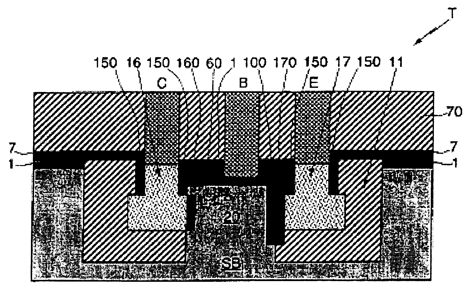
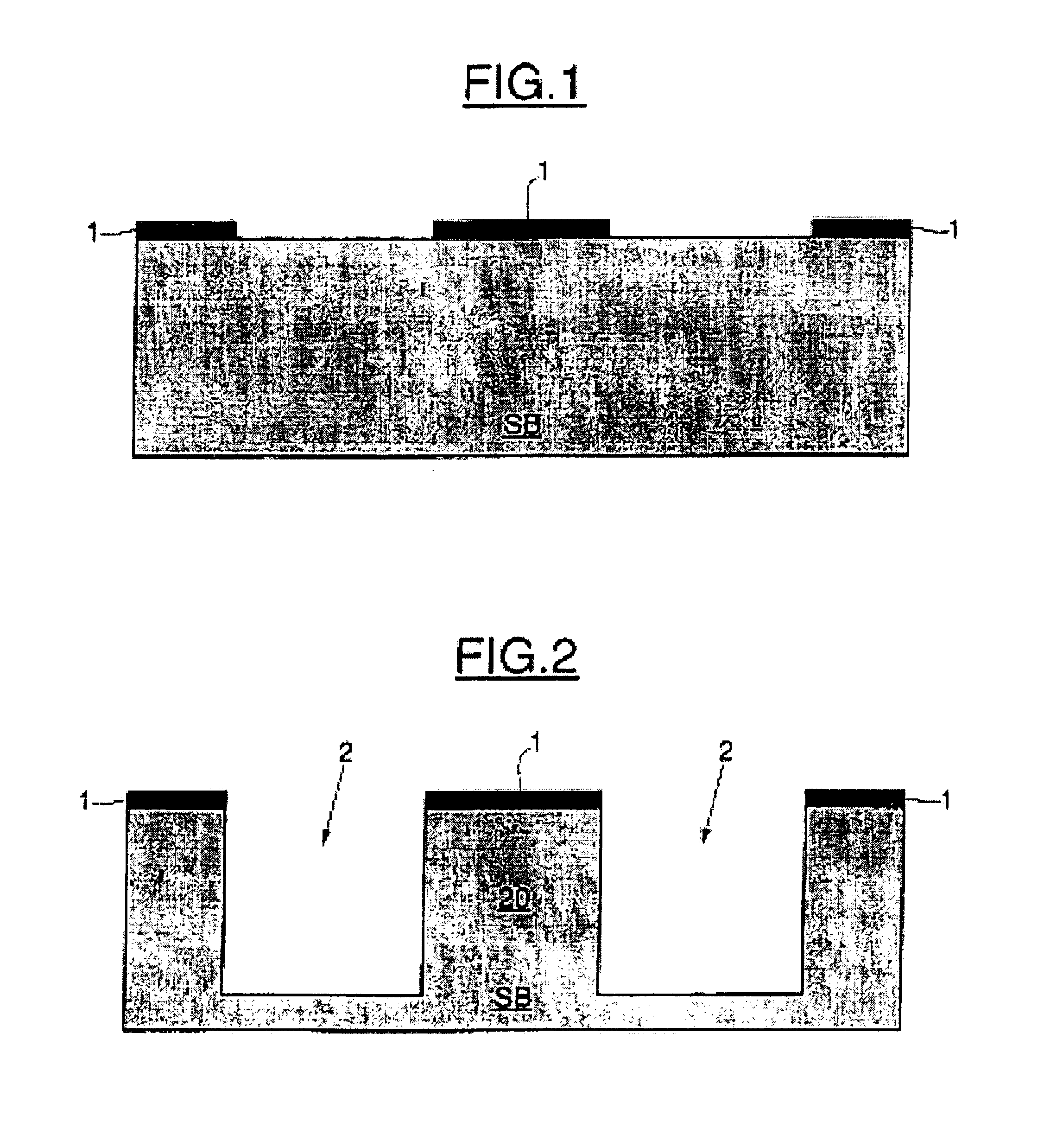
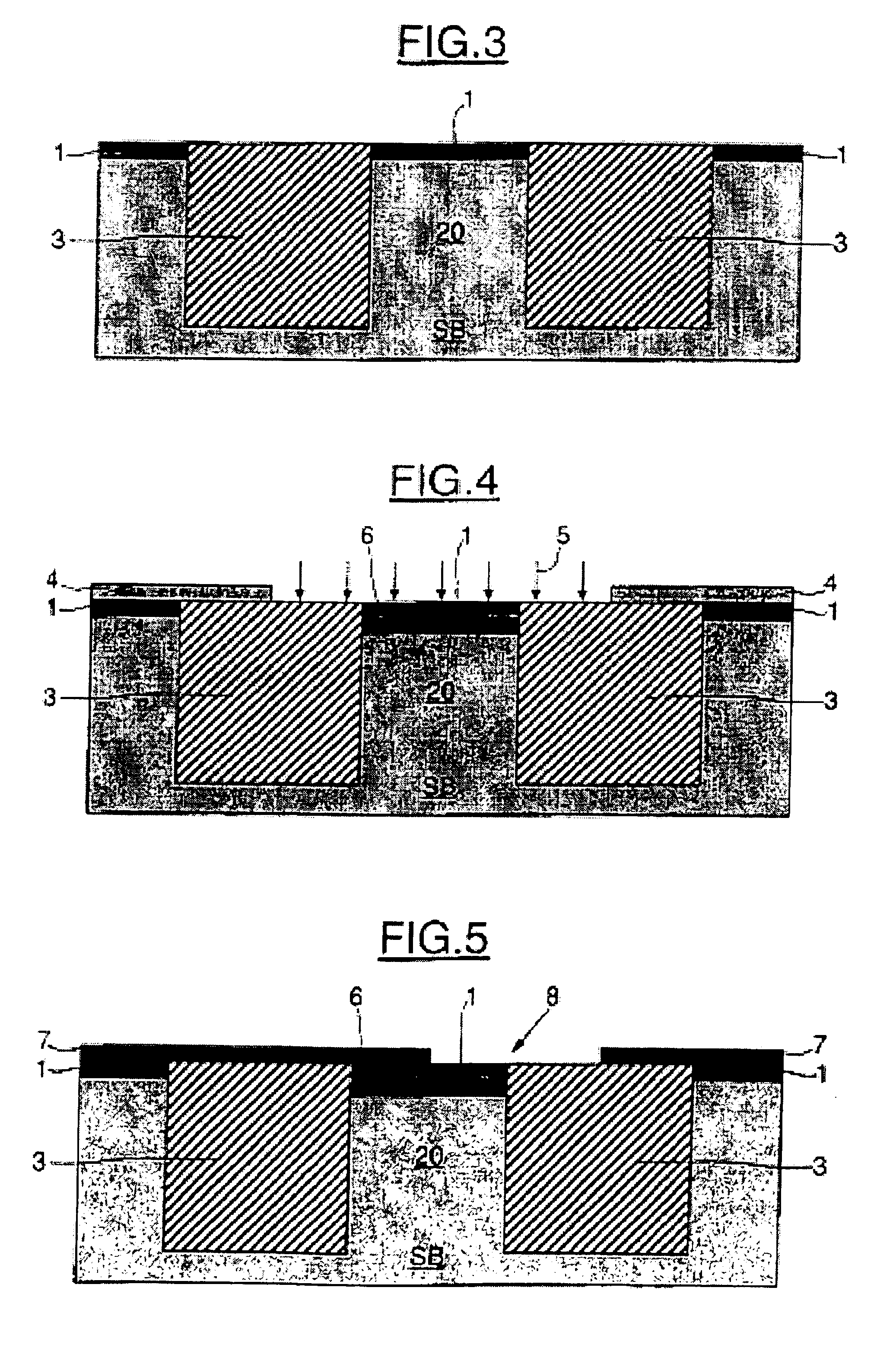
[0041]FIG. 1 shows a semiconductor bulk (substrate) SB, which is N-doped, for example, within which an NPN bipolar transistor according to the present invention is to be produced.

[0042]A mask 1, for example of silicon nitride, typically having a thickness from 50 to 400 Å, is formed on the top surface of the bulk SB in a conventional manner known in the art. The silicon nitride mask 1 defines the locations of the future isolating well i...


PUM


Abstract

The transistor includes an emitter region 17 disposed in a first isolating well 11, 150 formed in a semiconductor bulk. An extrinsic collector region 16 is disposed in a second isolating well 3, 150 formed in the semiconductor bulk SB and separated laterally from the first well by a bulk separator area 20. An intrinsic collector region is situated in the bulk separator area 20 in contact with the extrinsic collector region. An intrinsic base region 100 is formed which is thinner laterally than vertically and in contact with the intrinsic collector region and in contact with the emitter region through bearing on a vertical flank of the first isolating well facing a vertical flank of the second isolating well. An extrinsic base region 60 is formed which is substantially perpendicular to the intrinsic base region in the top part of the bulk separator area, and contact terminals C, B, E respectively in contact with the extrinsic collector region, the extrinsic base region, and the emitter region.

Description

CROSS REFERENCE TO RELATED APPLICATIONS[0001]This application is based upon and claims priority from prior French Patent Application No. 0106141, filed May 9, 2001, the disclosure of which is hereby incorporated by reference in its entirety.BACKGROUND OF THE INVENTION[0002]1. Field of the Invention[0003]The present invention relates to integrated circuits and more particularly to lateral operation bipolar transistors.[0004]2. Description of Related Art[0005]Bipolar transistors are used to obtain higher output currents than MOS transistors. At present bipolar transistors have a vertical structure, generally including a buried extrinsic collector layer on top of which is an intrinsic collector region formed in the semiconductor bulk (substrate). On top of the intrinsic collector region is a base region covered with an emitter block.[0006]Apart from the fact that these vertical structure, vertical operation bipolar transistors have a collector / bulk capacitance and a buried collector la...

Claims


Application Information

Patent Timeline
Patent Type & Authority Patents(United States)
IPC IPC(8): H01L29/06H01L29/10H01L29/02
CPCH01L29/1012H01L29/0649H01L29/735H01L29/6625H01L29/0653H01L29/1008
Inventor MENUT, OLIVIERJAOUEN, HERVE
Owner STMICROELECTRONICS SRL
Why Eureka
Try Eureka