Method and structure for improving the linearity of MOS switches

a linearity and mos switch technology, applied in the field ofmos switches, can solve the problems of harmonic distortion, input signal dependent switch on-resistance, gate-to-source voltage modulation of active switch, etc., and achieve the effect of improving the spurious free dynamic range (sfdr)

Inactive Publication Date: 2005-05-24
TEXAS INSTR INC
View PDF5 Cites 41 Cited by
  • Summary
  • Abstract
  • Description
  • Claims
  • Application Information

AI Technical Summary

Benefits of technology

[0010]The present invention is directed to a technique to linearize a MOS switch's on-resistance and the nonlinear junction capacitance. The technique linearizes the MOS switch by using a unity gain buffer with proper DC shift to drive a MOS bulk (back gate) to improve the spurious free dynamic range (SFDR). In this way, the 2nd-order effect such as body effect (VT(VSB)) and nonliner junction capacitance Cj(VSB)) can be substantially removed. The MOS front gate may or may not also be driven with a similar unity gain buffer having a different DC shift.

Problems solved by technology

The problem with a conventional sampling switch then is that the switch on-resistance is input signal dependent, and generates harmonic distortion.
As discussed herein before, distortion occurs due to the modulation of the gate-to-source voltage of the active switches caused by the switch source / drain node voltage varying with the input or feedback signal.
This known technique is still problematic however, in that a residual non-linearity remains due to the modulation of the source to bulk (back gate) voltage.

Method used


Image

  • Method and structure for improving the linearity of MOS switches
  • Method and structure for improving the linearity of MOS switches
  • Method and structure for improving the linearity of MOS switches

Examples


Embodiment Construction

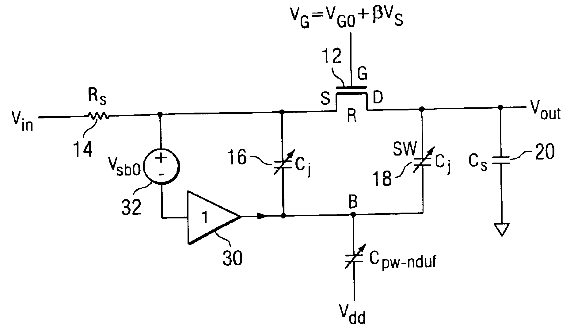
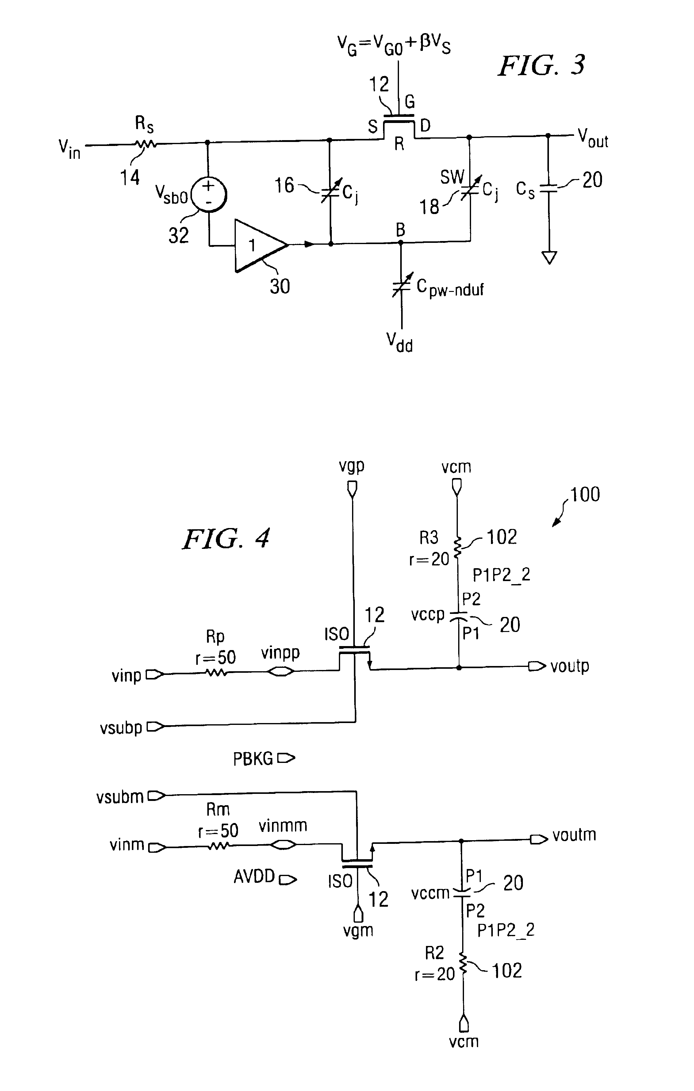
[0028]FIG. 3 illustrates a MOS switch 12 with a lumped RC model and a substantially unity gain buffer 30 driving a bulk terminal in order to remove the signal content from the source-to-bulk voltage VSB, and a DC voltage shifter 32 introduced to reverse bias the junction for limiting the junction capacitance size as well as its nonlinearity according to one embodiment of the present invention. The present inventors observed that both VT associated with body effect and Cj associated with junction capacitance, are VSB dependent. If the bulk terminal is driven with a buffer to track the input signal even with a reasonable amount of offset, VSB can be forced to be a constant. In this way both non-linear junction capacitance and nonlinear body effect are substantially removed. This technique is denoted herein after as the ‘dynamically biased bulk terminal technique’. The buffer 30 is used to drive the MOS bulk terminal in order to remove the signal content from VSB as stated herein befor...


PUM


Abstract

A technique is provided to linearize a MOS switch on-resistance and the nonlinear junction capacitance. The technique linearizes the sampling switch by using a buffer having substantially unity gain with proper DC shift to drive an isolated bulk terminal of the MOS well to improve the spurious free dynamic range (SFDR). In this way, the 2nd-order effect such as nonlinear body effect (VT(VSB)) and nonlinear junction capacitance (Cj(VSB)) can be substantially removed.

Description

BACKGROUND OF THE INVENTION[0001]1. Field of the Invention[0002]This invention relates generally to MOS switches, and more particularly, this invention relates to a technique to improve the linearity of a MOS switch beyond that achievable using known methods and structures.[0003]2. Description of the Prior Art[0004]MOS switches are commonly employed in both continuous time applications and sampling applications. Programmable gain amplifiers, for example, include MOS switches to select input and feedback resistors to achieve a desired gain. A typical sample and hold (S / H) circuit in a CMOS process employs two basic devices, a MOS switch and capacitor. The switch works in its triode region as a MOS resistor. Harmonic distortions (HDs) are generated when AC current charging the sampling capacitor Cs passes through the resistor whenever the capacitor and / or the resistor are nonlinear. As used herein, HD3 means third harmonic distortion.[0005]A S / H circuit 10 can be modeled as shown in F...

Claims


Application Information

Patent Timeline
Patent Type & Authority Patents(United States)
IPC IPC(8): H03K17/06G05F3/26G05F3/08
CPCH03K17/063G05F3/262
Inventor CHEN, FENGRICHARDSON, DONALD C.BETTY, CHRISTOPHER L.
Owner TEXAS INSTR INC
Why Eureka
Try Eureka