Differential circuit, amplifier circuit, and display device using the amplifier circuit

a technology of amplifier circuit and display device, which is applied in the direction of different amplifiers, amplifiers with semiconductor devices/discharge tubes, instruments, etc., to achieve the effect of wide input and output ranges and reduced power consumption

Inactive Publication Date: 2005-05-24
NEC LCD TECH CORP
View PDF12 Cites 15 Cited by
  • Summary
  • Abstract
  • Description
  • Claims
  • Application Information

AI Technical Summary

Benefits of technology

[0036]Accordingly, an object of the present invention is to provide a differential circuit and an amplifier circuit that enable wide input and output ranges, realize high-speed driving for both charging and discharging operations, and allow a reduction in power consumption, when driving a capacitive load.
[0037]Another object of the present invention is to provide a display device which achieves low power consumption through the use of the circuit described above for a data line driver circuit in the display device.
[0041]Accordingly, in the present invention, in order to solve the problems described above, changeover of a polarity symmetry of the differential circuit is made according to whether charging or discharging on the output terminal is performed, thereby allowing direct control over the gate voltages of the transistors for charging and discharging the output terminal by the output signal of the differential circuit. Incidentally, a method is feasible where two polarity symmetric differential circuits are provided separately and according to whether charging or discharging on the output terminal is performed, selection between the two polarity symmetric differential circuits is performed. The number of devices, however, increases greatly, and an area of the devices also increases. On contrast therewith, the present invention solves the problems described above by a space saving differential circuit configuration where an increase in the number of devices is small.

Problems solved by technology

The problem described above is ascribable to the fact that the gate voltage of the NMOS transistor for discharging the output terminal (2) cannot be directly controlled by the output signal of the differential circuit, while the gate voltage of the PMOS transistor for charging the output terminal (2) can be directly controlled by the output signal of the differential circuit.

Method used


Image

  • Differential circuit, amplifier circuit, and display device using the amplifier circuit
  • Differential circuit, amplifier circuit, and display device using the amplifier circuit
  • Differential circuit, amplifier circuit, and display device using the amplifier circuit

Examples


first embodiment

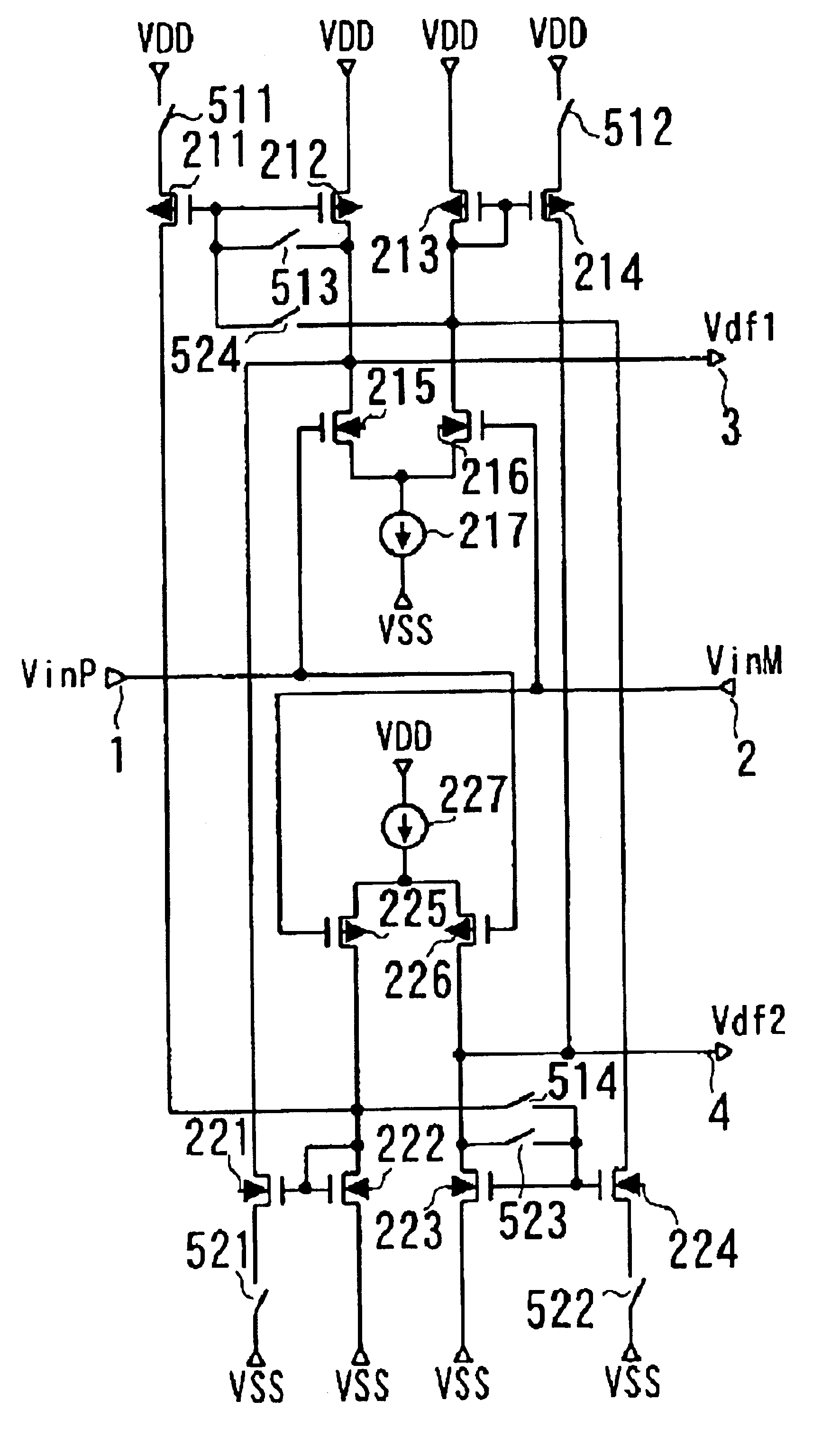
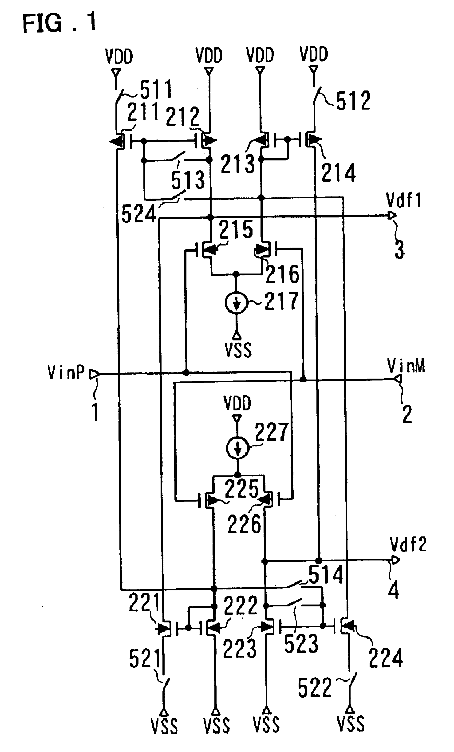
[0163]In order to describe the mode for practicing the present invention in further detail, embodiments of the present invention will be described with reference to drawings. FIG. 1 is a diagram showing the present invention.

[0164]Referring to FIG. 1, a differential circuit according to this embodiment includes n-channel transistors 215 and 216, p-channel transistors 211, 212, 213 and 214, a constant-current source 217 and switches 511, 512, 513 and 524 and outputs a first differential output Vdf1 from a drain of the n-channel transistor 215.

[0165]Sources of the n-channel transistors 215 and 216 are commonly connected to the constant-current source 217, and the n-channel transistors 215 and 216 receive input voltages VinP and VinM at their gates, respectively to form a differential pair. The source of the p-channel transistor 212 is connected to a power supply VDD, and a drain of the p-channel transistor 212 is connected to the drain of the n-channel transistor 215. The source of th...

third embodiment

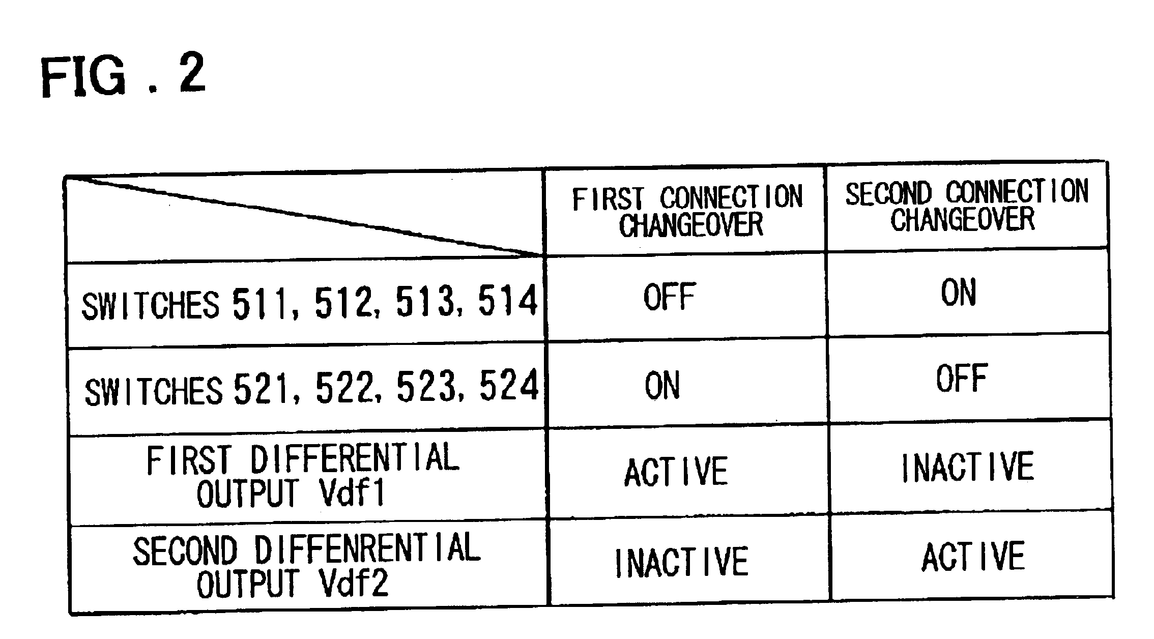
[0198]Next, other embodiment of the present invention will be described. FIG. 6 shows a configuration according to the present invention. FIG. 6 shows the configuration of an amplifier circuit configured by using the differential circuit in FIG. 1. That is, a differential circuit in FIG. 6 including the n-channel differential pair (215, 216), p-channel differential pair (225, 226), p-channel transistors (211, 212, 213, 214), n-channel transistors (221, 222, 223, 224), constant-current sources 217 and 227, and connection changeover means (the switches 511 to 514, 521 to 524) is the same as the differential circuit shown in FIG. 1. FIG. 7 is a table showing an example of methods of controlling the amplifier circuit in FIG. 6.

[0199]Referring to FIG. 6, this amplifier circuit is a feedback-type amplifier circuit that includes amplification stages 310 and 320 that operate in response to the outputs Vdf1 and Vdf2 of the differential circuit shown in FIG. 1, respectively. Referring to FIG....

fourth embodiment

[0207]Other embodiment of the present invention will also be described. FIG. 8 shows a configuration according to the present invention. FIG. 8 shows the configuration of an amplifier circuit configured by using the differential circuit in FIG. 1. That is, referring to FIG. 8, an amplifier circuit 210 composed by the n-channel differential pair (215, 216), p-channel differential pair (225, 226), p-channel transistors (211, 212, 213, and 214), n-channel transistors (221, 222, 223, and 224), constant-current sources 217 and 227, and connection changeover means (the switches 511 to 514, 521 to 524) is the same as the differential circuit shown in FIG. 1.

[0208]The amplification stage 310 for charging includes a p-channel transistor 311, a switch 553, and a constant-current source 313. The source of the p-channel transistor 311 is connected to the high-potential power supply VDD, the drain of the p-channel transistor 311 is connected to the output terminal 2, and the gate of the p-channe...


PUM


Abstract

A differential circuit comprises first and second differential pairs driven by constant-current sources, respectively, for receiving input voltages, first transistors, second transistors, and switches are included. In a first connection state, one current mirror comprises among the first transistors. Input and output terminals of the one current mirror are connected to outputs of the first differential pair. Two current mirrors are composed by the second transistors. Inputs of the two current mirrors are connected to the outputs of the second differential pair, and the outputs of the two current mirrors are connected to an input and an output of the one current mirror circuit. The output of the one current mirror is a first output. In a second connection state, one current mirror comprises among the second transistors. The input and the output of the one current mirror are connected to the outputs of the second differential pair. Two current mirrors are composed by the first transistors. The inputs of the two current mirrors are connected to the outputs of the first differential pair, and the outputs of the two current mirror circuits are connected to the input and the output of the one current mirror circuit, respectively. The output terminal of the one current mirror is a second output terminal.

Description

FIELD OF THE INVENTION[0001]The present invention relates to a differential circuit, an amplifier circuit, and a display device including the amplifier circuit.BACKGROUND OF THE INVENTION[0002]As an operational amplifier that enables wide input and output ranges, the operational amplifier with the wide input and output ranges as shown in FIG. 17 is disclosed in JP Patent Kokai Publication JP-A-5-63464. The operational amplifier in FIG. 17 is comprised of a differential circuit 910 and an output stage 950. In the differential circuit 910, a current mirror circuit composed by PMOS transistors (912, 913) (referred to as a “PMOS current mirror circuit”) is connected as a load circuit to outputs of a differential pair of NMOS transistors (915, 916) (also referred to an “NMOS differential pair), driven by a current source 917. Further, input terminals of two pairs of current mirror circuits composed by NMOS transistors (referred to as “NMOS current mirror circuits”) are respectively conne...

Claims


Application Information

Patent Timeline
Patent Type & Authority Patents(United States)
IPC IPC(8): H03F3/45G09G3/20G09G3/36H03F3/68
CPCH03F3/4521H03F2203/45726
Inventor TSUCHI, HIROSHI
Owner NEC LCD TECH CORP
Why Eureka
Try Eureka