Phase dislocation control single-stage power factor correction control circuit and switching power supply
A power factor correction and control circuit technology, applied in the direction of control/regulation system, high-efficiency power electronic conversion, output power conversion device, etc., can solve the problem of excessive bus current ripple, output power reduction, input current ripple, etc. problem, achieve the effect of reducing ripple current, reducing peak value and effective value, and low circuit cost
- Summary
- Abstract
- Description
- Claims
- Application Information
AI Technical Summary
Problems solved by technology
Method used
Image
Examples
Embodiment 1
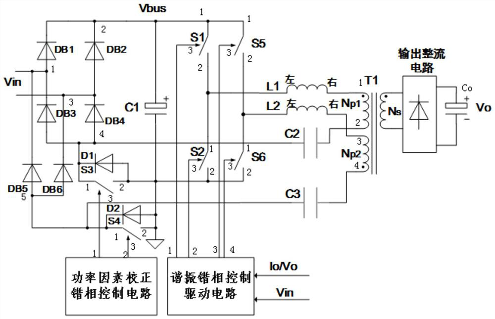
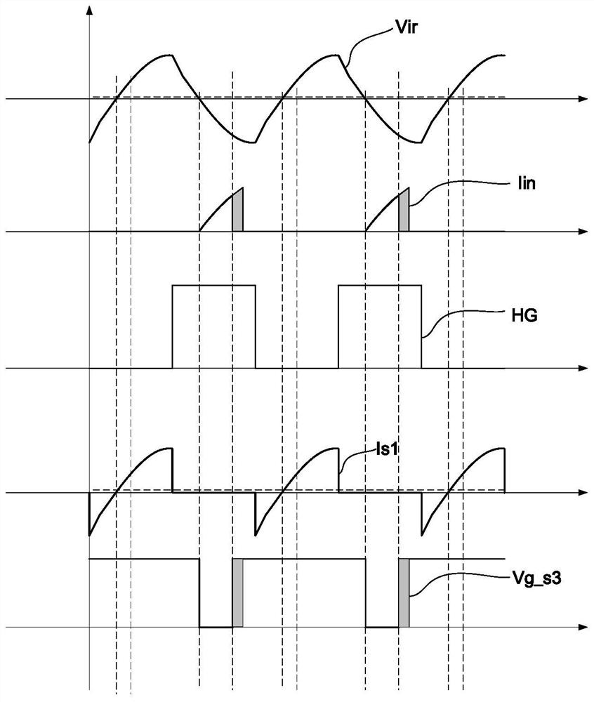
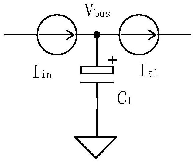
[0032] Now in conjunction with accompanying drawing and specific embodiment the present invention is further described, as figure 1As shown, the single-stage power factor correction control circuit with phase error control according to the embodiment of the present invention includes grid input Vin, rectifier bridge DB, capacitor C1, capacitor C2, capacitor C3, switch tube S1, switch tube S2, switch tube S3, Switch tube S4, switch tube S5, switch tube S6, diode D1, diode D2, inductor L1, inductor L2, transformer T1, first output rectifier circuit, output capacitor Co, power factor correction phase error control circuit and resonance phase error control drive circuit; the grid input Vin is connected to the first end and the third end of the rectifier bridge DB, and the second end of the rectifier bridge DB is connected to the positive pole of the capacitor C1, the first end of the switch tube S1 and the The first end of the switching tube S5 is connected, the second end of the ...
Embodiment 2
[0041] Such as Figure 4 As shown, the single-stage power factor correction control circuit according to the embodiment of the present invention includes a grid input Vin, a rectifier bridge DB, a capacitor C1, a capacitor C2, a capacitor C3, a capacitor C4, a switch tube S1, a switch tube S2, and a switch Tube S3, switch tube S4, switch tube S5, switch tube S6, switch tube S7, diode D1, diode D2, inductor L1, inductor L2, transformer T1, first output rectifier circuit, second output rectifier circuit, output capacitor Co, Current transformer CT1, capacitor C3, power factor correction out-of-phase control circuit and resonant out-of-phase control drive circuit; wherein, the grid input Vin is connected to the first end and the third end of the rectifier bridge DB, and the rectifier bridge The second end of DB is sequentially connected to the positive pole of the capacitor C1, the first end of the switch tube S1 and the first end of the switch tube S5, and the second end of the ...
PUM
 Abstract
Description
Claims
Application Information


