

Ultra violet ray photo detector based on gallium nitride semiconductor
A photodetector and ultraviolet technology, which is applied in semiconductor devices, photometry, and electrical solid state devices, can solve problems such as excessive differences in lattice constants, affecting performance, and poor epitaxy structures.
- Summary
- Abstract
- Description
- Claims
- Application Information
AI Technical Summary
Problems solved by technology
Method used
Image

Examples
Embodiment Construction
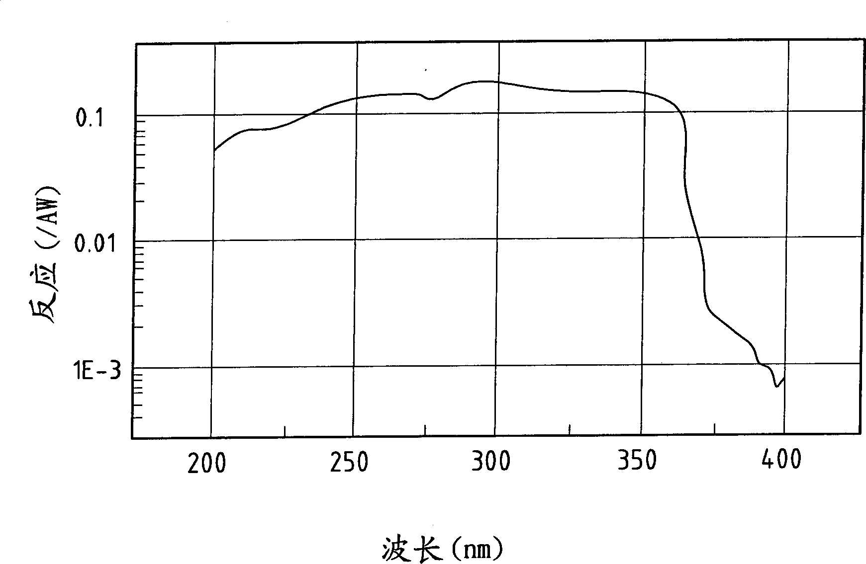
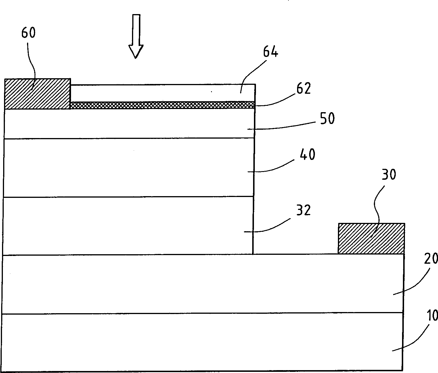
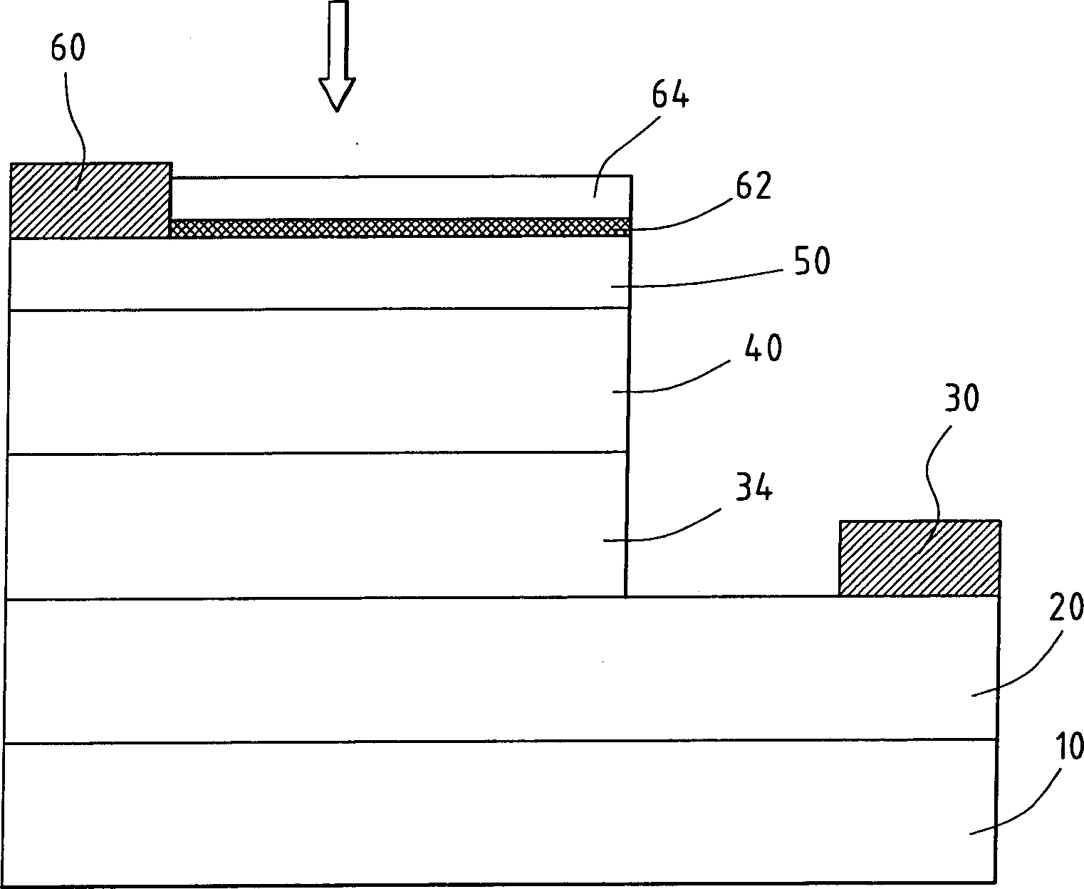
[0028] figure 2 is a schematic diagram of the first embodiment of the ultraviolet photodetector structure of the present invention. Such as figure 2 As shown, this embodiment uses C-Plane, R-Plane or A-Plane alumina single crystal (Sapphire) or silicon carbide (6H-SiC or 4H-SiC) as the substrate 10, and other materials that can be used for the substrate 10 Also includes Si, ZnO, GaAs or spinel (MgAl 2 o 4 ), or a single crystal oxide whose lattice constant is close to that of a nitride semiconductor, and then an n-type contact layer 20 is formed on one side of the substrate 10. The n-type contact layer 20 is made of n-type doped and has a specific composition Al a Ga b In 1-a-b N (0≤a, b≤1, a+b≤1), the thickness is between 3000 Å and 40000 Å, and the growth temperature is between 700°C and 1200°C. Then, a light absorbing layer 32 is formed on the n-type contact layer 20, and the light absorbing layer 32 is made of undoped Al with a specific composition. c Ga d In 1...
PUM
 Abstract
Description
Claims
Application Information