Single crystal production method

a production method and single crystal technology, applied in the direction of crystal growth process, polycrystalline material growth, under protective fluid, etc., can solve the problems of product yield lowering, product yield lowering, and crystal cannot be used as a substrate for a semiconductor device, so as to improve the product yield

Inactive Publication Date: 2005-05-31
SILTRONIC AG
View PDF5 Cites 5 Cited by
  • Summary
  • Abstract
  • Description
  • Claims
  • Application Information

AI Technical Summary

Benefits of technology

[0009]The object of the present invention is to improve the product yield by pr...

Problems solved by technology

Namely, the surface of the melt may be waved due to mechanical vibrations, the crystal may be dislocated or become polycrystalline due to increase of the temperature fluctuations accompanying the waves, so that the crystal cannot be used as a substrate for a semiconductor device.
And, even if the crystal can avoid these problems, the crystal is likely to undergo deformation of the crystal shape and the product yield may be lowered because the crystal does not take a predetermined shape.
Further, in case of a ...

Method used


Image

  • Single crystal production method
  • Single crystal production method
  • Single crystal production method

Examples


embodiment 1

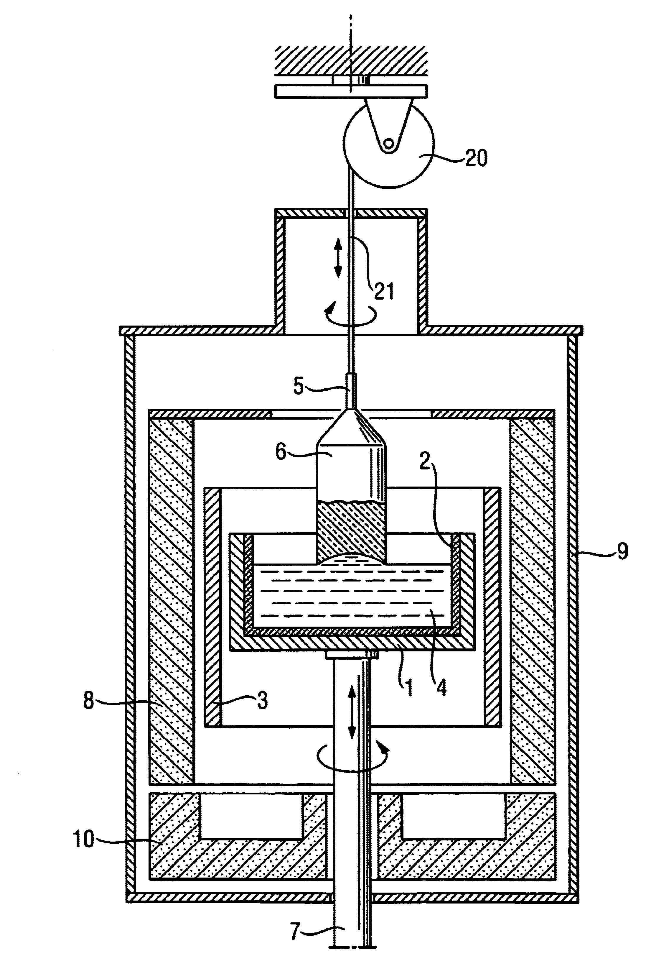
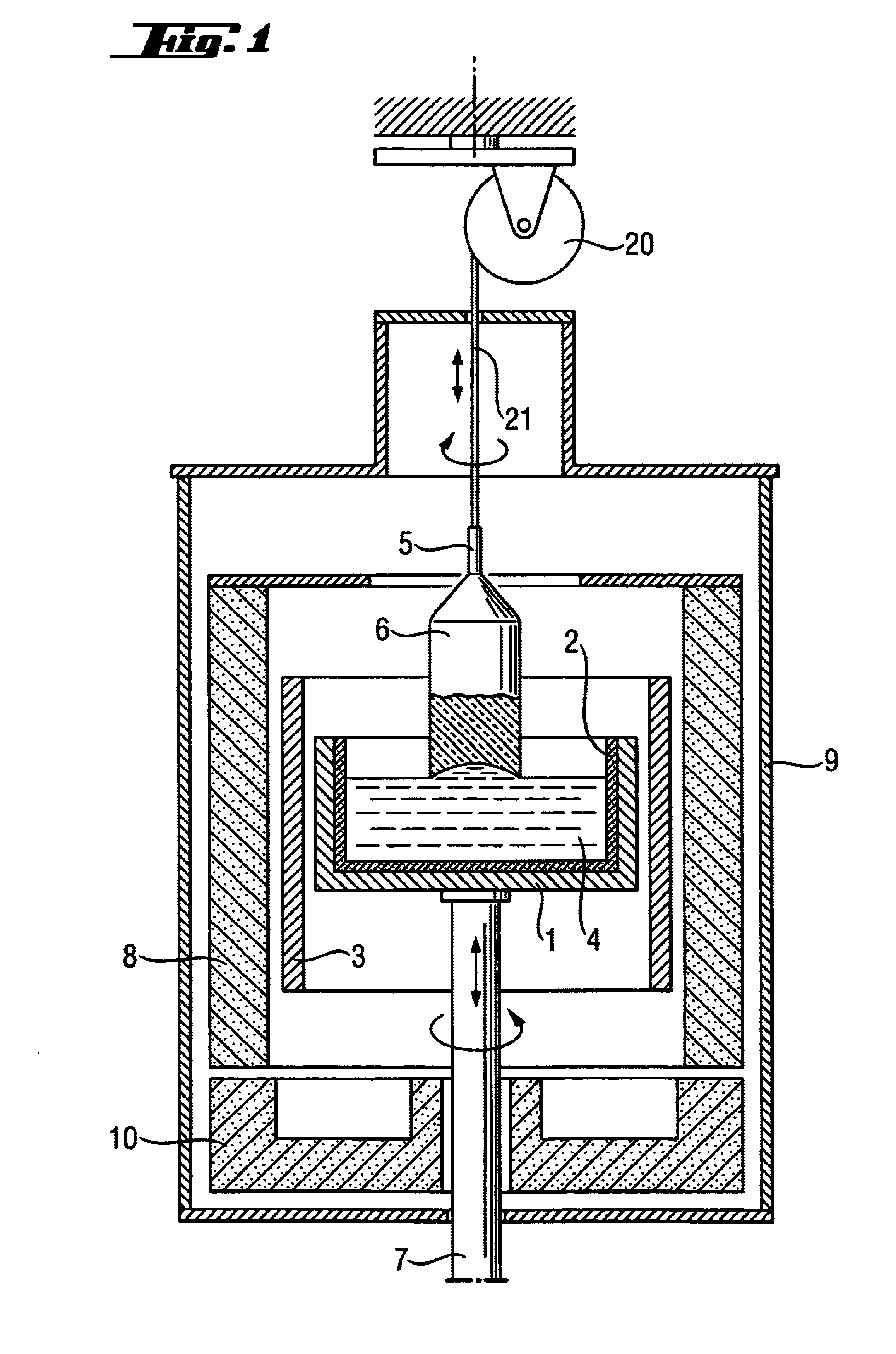
[0027]The silicon raw material of 20 kg is molten in a cylindrical crucible having an inner diameter of 150 mm and a depth of 150 mm, and a silicon single crystal is grown with the use of the seed crystal having the (100) orientation. The crystal is grown in such a manner that the crucible is revolved at the predetermined number of rotations of 10 rpm and the crystal is revolved at the number of rotations of 20 rpm in a direction opposite to the crucible, from the time when the seed crystal is dipped into the melt till the quantity of the melt reaches 13 kg. At this time, since the orientation of the seed crystal is (100), four projections due to the crystal habit lines each being approximately identical in size are formed at the edge of the growing interface of the crystal. And, the melt in the crucible has been continuously vibrated mainly with the number of vibrations as 120 rpm.

[0028]From the time when the quantity of the melt reaches 12.5 kg, as shown in Table 1, by reducing th...

embodiment 2

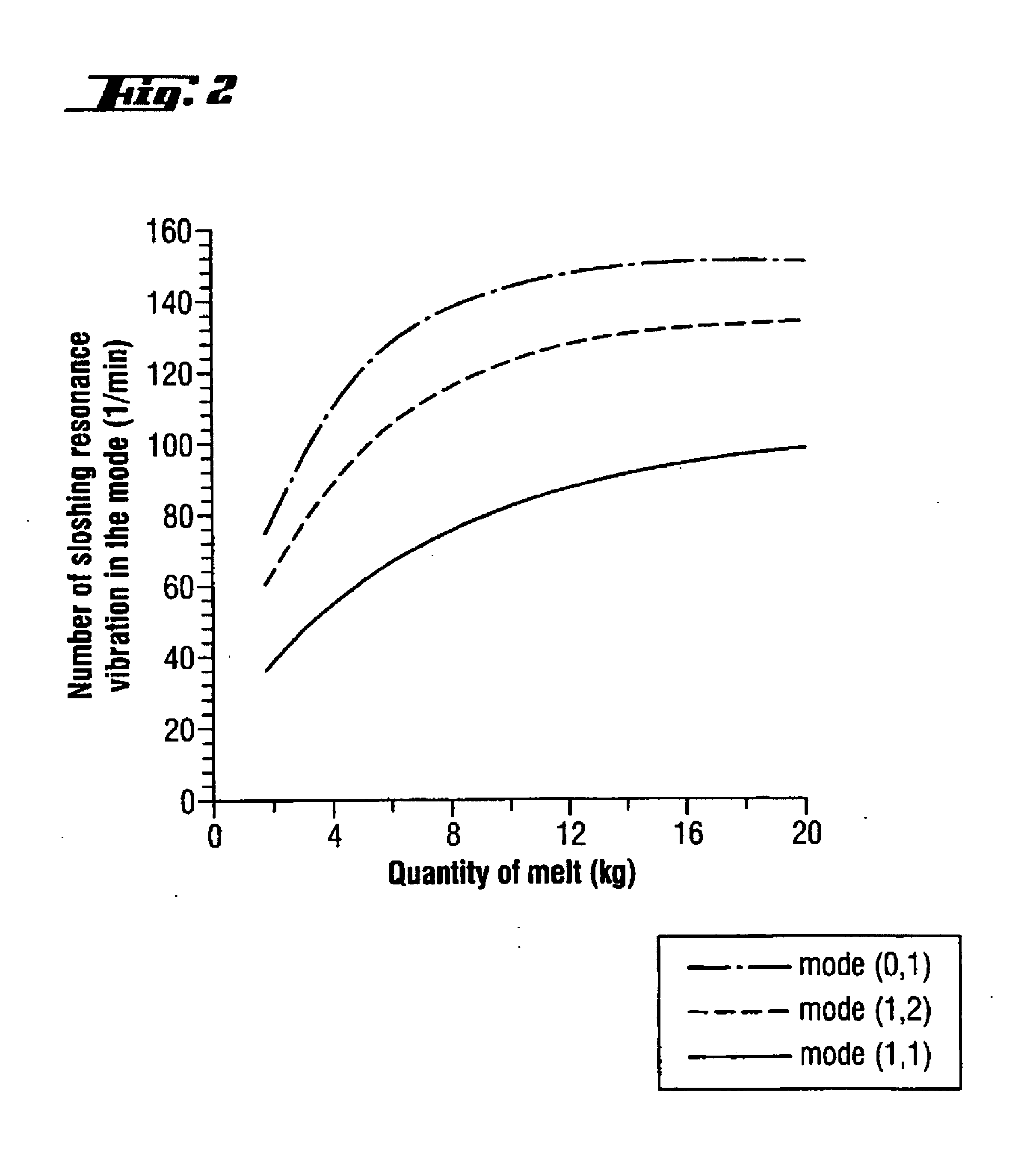
[0032]The raw material of 20 kg is molten in the cylindrical crucible having an inner diameter of 150 mm and a depth of 150 mm to grow a silicon single crystal with the use of the seed crystal having the (100) orientation. The crystal is grown in the following manner: the crucible is rotated at 10 rpm from the time when the seed crystal is dipped into the melt till the quantity of the melt reaches 12.5 kg, and the crystal is rotated at 20 rpm in a direction opposite to the crucible. At this time, the number of vibrations of the melt driven by the crystal is 120 rpm. When the quantity of the melt reaches 12.5 kg, the number of sloshing resonance vibrations in the mode (1,2) approaches 93% of the number of vibrations of the melt driven by the crystal.

[0033]Therefore, the number of rotations of the crystal and crucible are increased to 22 rpm and 12 rpm, respectively for 15 minutes (i.e. the time corresponding to the number of vibrations of the melt due to the sloshing, 1930=128.7 rpm×...


PUM


Abstract

A single crystal production method based on the Czochralski method comprises controlling a number of crucible rotations and crystal rotations so that a number of vibrations for driving a melt, determined on the basis of the number of crucible and crystal rotations during a single crystal growing procedure, is outside a range from 95% to 105% of a number of sloshing resonance vibrations of the melt. In another embodiment, the method comprises controlling a number of rotations of a crystal and crucible, so that when a number of vibrations for driving a melt, determined by the number of crucible and crystal rotations during a single crystal growing procedure, is within a range from 95% to 105% of a number of sloshing resonance vibrations of the melt, the number of vibrations of the melt due to sloshing does not exceed 2000 times during a period when the number of vibrations is within that range.

Description

BACKGROUND OF THE INVENTION[0001]1. Field of the Invention[0002]The present invention relates to a single crystal production method based on the Czochralski method and more specifically, to a method for preventing a crystal from being dislocated, becoming polycrystalline and being deformed due to waves on the surface of a melt.[0003]2. The Prior Art[0004]While crystals of various element semiconductors and compound semiconductors have been used as a substrate for making electronic devices and photoelectric devices, the Czochralski method is used for producing these crystals. The Czochralski method is useful for producing large crystals, and most silicon single crystals in the current semiconductor device fabrication are produced by means of the Czochralski method.[0005]FIG. 1 is a longitudinal sectional view of a crystal puller as a model, based on the Czochralski method. In this crystal puller, a melt 4 is obtained by filling with the crystal raw material a crucible 2 housed in a s...

Claims


Application Information

Patent Timeline
IPC IPC(8): C30B15/30C30B15/00C30B29/06C30B15/20
CPCC30B15/30C30B29/06Y10T117/1068Y10T117/1072C30B15/20
Inventor KISHIDA, YUTAKATAMAKI, TERUYUKITAKEBAYASHI, SEIKIOHASHI, WATARU
Owner SILTRONIC AG
Why Eureka
Try Eureka