Conductive thin film for semiconductor device, semiconductor device, and method of manufacturing the same

a technology of conductive thin film and semiconductor device, which is applied in the direction of semiconductor device, semiconductor/solid-state device details, electrical apparatus, etc., can solve the problems of easy corrosion of cr, deterioration of device performance, and high electric resistance and the like, so as to improve the dispersibility of mo, simplify the process of depositing mo/al/mo, and improve the dispersion of mo

Inactive Publication Date: 2005-05-31
IDEMITSU KOSAN CO LTD
View PDF11 Cites 78 Cited by
  • Summary
  • Abstract
  • Description
  • Claims
  • Application Information

AI Technical Summary

Benefits of technology

[0016]By forming a gate electrode and / or a source / drain electrode from the conductive thin film, even when an electrode wire is in direct contact with a silicon layer, diffusion of metal atoms into the silicon layer can be prevented, so that the performance of a semiconductor device obtained does not deteriorate.
[0031]According to the method, adhesiveness of the gate electrode and the source / drain electrode to a substrate (for example, glass substrate) and a silicon layer (such as silicon nitride film, semiconductor layer, or silicon wafer) is high and peeling does not occur during a manufacturing process. Thus, a semiconductor can be manufactured stably.

Problems solved by technology

Although Cr is easily processed, there is a problem that Cr is easily corroded.
Although TaW is resistive to corrosion and the like, it has a problem of high electric resistance and the like.
However, when an aluminum electrode is in direct contact with a silicon layer and a drive electrode, problems occur such that aluminum is diffused into the silicon layer, thereby deteriorating device performance, and aluminum is oxidized and converted into alumina, it increases the electric resistance with the drive electrode, and the device does not operate normally.
Consequently, there is a drawback that the process is complicated.
However, silver and copper have low adhesion to with a silicon nitride film, a silicon wafer, or the like which is made of glass or an insulating film.
It causes a problem such that silver and copper come off during the manufacturing process.

Method used


Image

  • Conductive thin film for semiconductor device, semiconductor device, and method of manufacturing the same
  • Conductive thin film for semiconductor device, semiconductor device, and method of manufacturing the same

Examples


example 1

[0056]A sputtering target obtained by opening a hole of 10 mmφ in an Ag target of 1.4 inches φ and inserting an Mo target of 10 mmφ into the hole was used and a thin film having a film thickness of 2,000 Å was formed on a silicon wafer by DC magnetron sputtering at a substrate temperature of 300° C. The content of Mo in the thin film was 5.1% by weight and resistivity was 2.4 μΩ·cm. Adhesion strength by a scratch test of the thin film was 5.57N. The scratch test was conducted as follows.

(1) Measurement Principle

[0057]A coated substrate is scratched with a diamond cone at constant speed while increasing a load at constant speed, and a destruction which occurs in or on the thin film is detected by an AE sensor. By using a load at which an AE signal rapidly goes high as a critical load, a quantitative value of adhesion strength is obtained.

[0058]By observing the surface after the scratch, a load of destruction (interface peel, film base material destruction, and the like) in a predeter...

examples 2 to 4

[0067]Thin films were formed in a manner similar to Example 1 except that the content of Mo and the content of the third metal in the sputtering target were changed as shown in Table 1, and evaluation was made. The results are shown in Table 1.

example 5

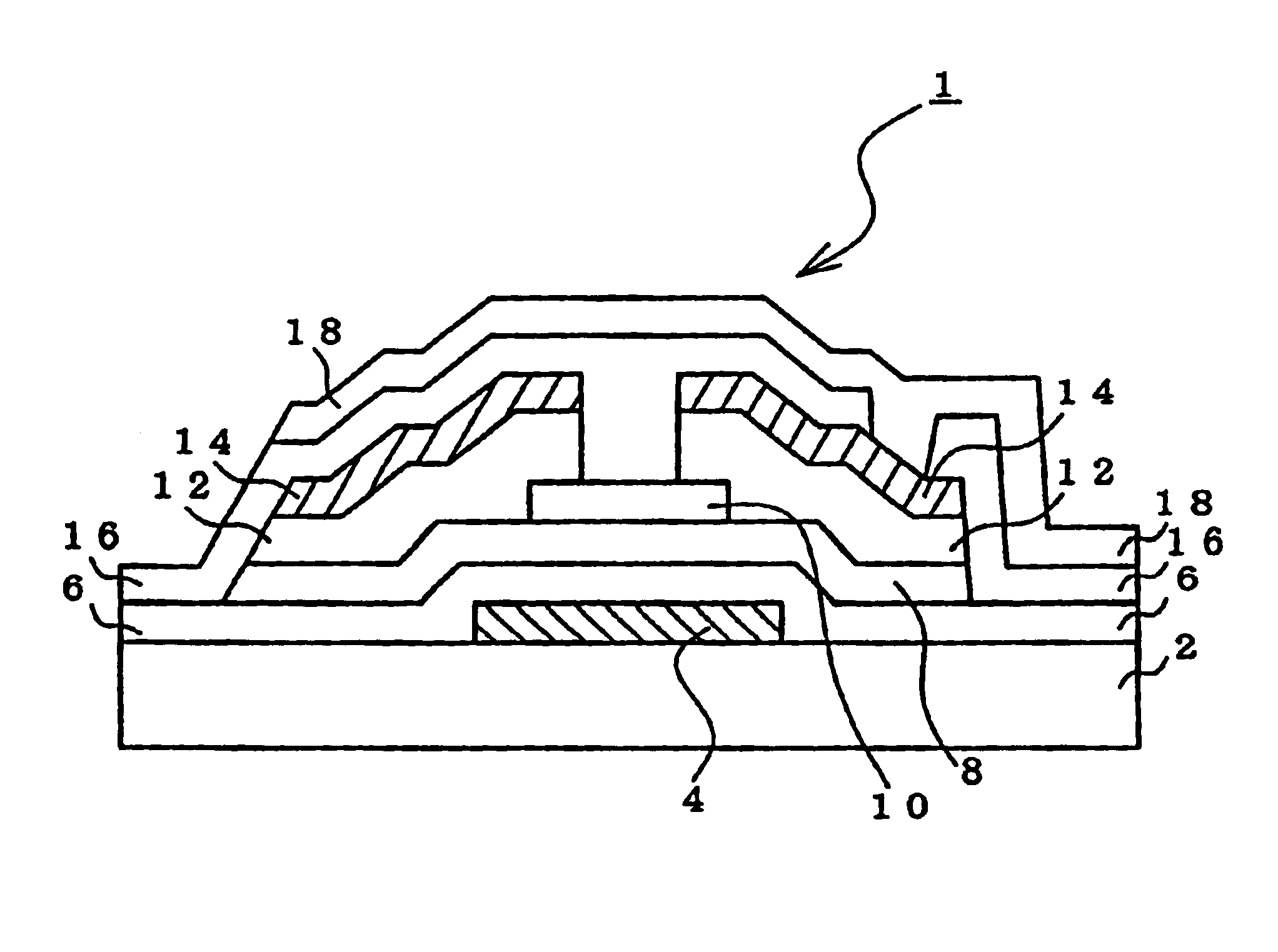
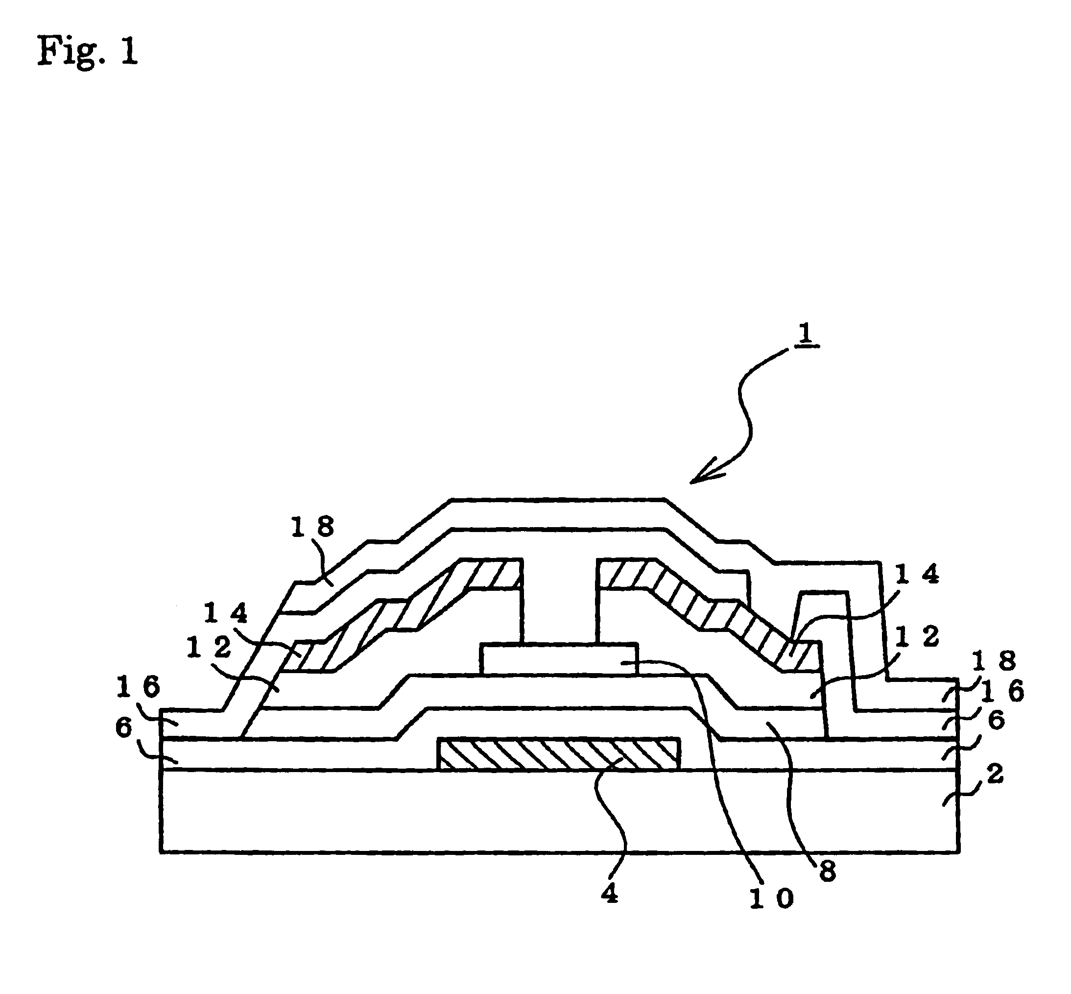
[0070]An embodiment of the invention will be described by using FIG. 1.

[0071]FIG. 1 is a cross sectional view showing an embodiment of a semiconductor device of the invention.

[0072]On a light transmittable glass substrate 2, a metal Ag (resistivity: 2.4 μΩ·cm) containing 5% by weight of Mo was deposited to a film thickness of 2,500 Å by high frequency sputtering. The layer was subjected to photoetching using a nitric acid-acetic acid-phosphoric acid solution as an etchant, thereby forming a gate electrode 4 (gate electrode wire) of a desired shape.

[0073]Next, a gate insulating film 6 as a first silicon nitride (SiNx) film (silicon layer) was deposited to a film thickness of 3,000 Å.

[0074]Subsequently, a SiH4—N2 mixed gas was used as a discharge gas and an α-Si:H(i) film (silicon layer) 8 was deposited to a film thickness of 3,500 Å.

[0075]Further, on the α-Si:H(i) film 8, by using an SiH4—NH3—N2 mixed gas as a discharge gas, a second silicon nitride (SiNx) film was deposited to a fil...


PUM


Abstract

A semiconductor device 1 obtained by depositing, on a substrate 2, a gate electrode 4 formed by a conductive thin film containing Mo atoms and Ag atoms, a gate insulating film 6, an α-Si:H(i) film 8, a channel protection layer 10, an α-Si:H(n) film 12, a source / drain electrode 14 formed by a conductive thin film containing Mo atoms and Ag atoms, a source / drain insulating film 16, and a drive electrode 18. By using a conductive thin film containing Mo atoms and Ag atoms, the gate electrode 4 and the source / drain electrode 14 are formed to manufacture the semiconductor device 1. Thus, the conductive thin film for a semiconductor device, having high adhesion strength to a substrate, an insulating layer, and the like, a semiconductor device which operates stably without deteriorating the performance, and a method of efficiently manufacturing the conductive thin film and the semiconductor device can be provided.

Description

[0001]This Application is a 371 of PCT / JP02 / 04556 May 10, 2002.TECHNICAL FIELD[0002]The present invention relates to a conductive thin film for a semiconductor device such as a semiconductor transistor, a semiconductor device, and a method of manufacturing the same.BACKGROUND ART[0003]A TFT is a very important component as a main component of a display of a portable personal computer, a laptop personal computer, a television, or the like.[0004]Companies manufacture TFTs by their methods. Since the process of manufacturing a TFT is complicated and various metals and metal oxides are deposited a plurality of times, simplification of the process is demanded.[0005]In a process of manufacturing a conventional TFT array, as materials of a gate electrode and a source / drain electrode, metals such as Cr and TaW are used.[0006]Although Cr is easily processed, there is a problem that Cr is easily corroded. Although TaW is resistive to corrosion and the like, it has a problem of high electric r...

Claims


Application Information

Patent Timeline
Patent Type & Authority Patents(United States)
IPC IPC(8): H01L21/336H01L21/02H01L29/45H01L29/49H01L29/40H01L21/285H01L21/288H01L29/786
CPCH01L21/2855H01L21/28568H01L21/32051H01L23/53247H01L29/458H01L29/4908H01L29/66765H01L2924/0002H01L2924/00H01L29/786
Inventor INOUE, KAZUYOSHIMATSUZAKI, SHIGEO
Owner IDEMITSU KOSAN CO LTD
Why Eureka
Try Eureka