Conductive thin film for semiconductor device, semiconductor device, and method of manufacturing the same

Inactive Publication Date: 2004-02-19
IDEMITSU KOSAN CO LTD
View PDF4 Cites 5 Cited by
  • Summary
  • Abstract
  • Description
  • Claims
  • Application Information

AI Technical Summary

Benefits of technology

0028] By forming a film by sputtering, a process of depositing Mo/Al/Mo, Ti/Al/Ti or the like can be simplified and a semiconductor device can be manufactured efficiently.
0029] By using a sputtering target mainly made of Ag to which an Mo compound such as an Mo/Al compound, an Mo/Be compound, an Mo/Ga compound, an Mo/Ge compound, an Mo/Ir compound, an Mo/Pt compound, an Mo/Re compound, an Mo/Si compound, an MoW alloy, an MoTa alloy, or an MoR

Problems solved by technology

Although Cr is easily processed, there is a problem that Cr is easily corroded.
Although TaW is resistive to corrosion and the like, it has a problem of high electric resistance and the like.
However, when an aluminum electrode is in direct contact with a silicon layer and a drive electrode, problems occur such that aluminum is diffused into the silicon layer, thereby deteriorating device performance, and aluminum is oxidized and c

Method used


Image

  • Conductive thin film for semiconductor device, semiconductor device, and method of manufacturing the same
  • Conductive thin film for semiconductor device, semiconductor device, and method of manufacturing the same

Examples


example 1

[0058] A sputtering target obtained by opening a hole of 10 mm.phi. in an Ag target of 1.4 inches .phi. and inserting an Mo target of 10 mm.phi. into the hole was used and a thin film having a film thickness of 2,000 .ANG. was formed on a silicon wafer by DC magnetron sputtering at a substrate temperature of 300.degree. C. The content of Mo in the thin film was 5.1% by weight and resistivity was 2.4 .mu..OMEGA..multidot.cm. Adhesion strength by a scratch test of the thin film was 5.57N. The scratch test was conducted as follows.

[0059] (1) Measurement Principle

[0060] A coated substrate is scratched with a diamond cone at constant speed while increasing a load at constant speed, and a destruction which occurs in or on the thin film is detected by an AE sensor. By using a load at which an AE signal rapidly goes high as a critical load, a quantitative value of adhesion strength is obtained.

[0061] By observing the surface after the scratch, a load of destruction (interface peel, film bas...

example 5

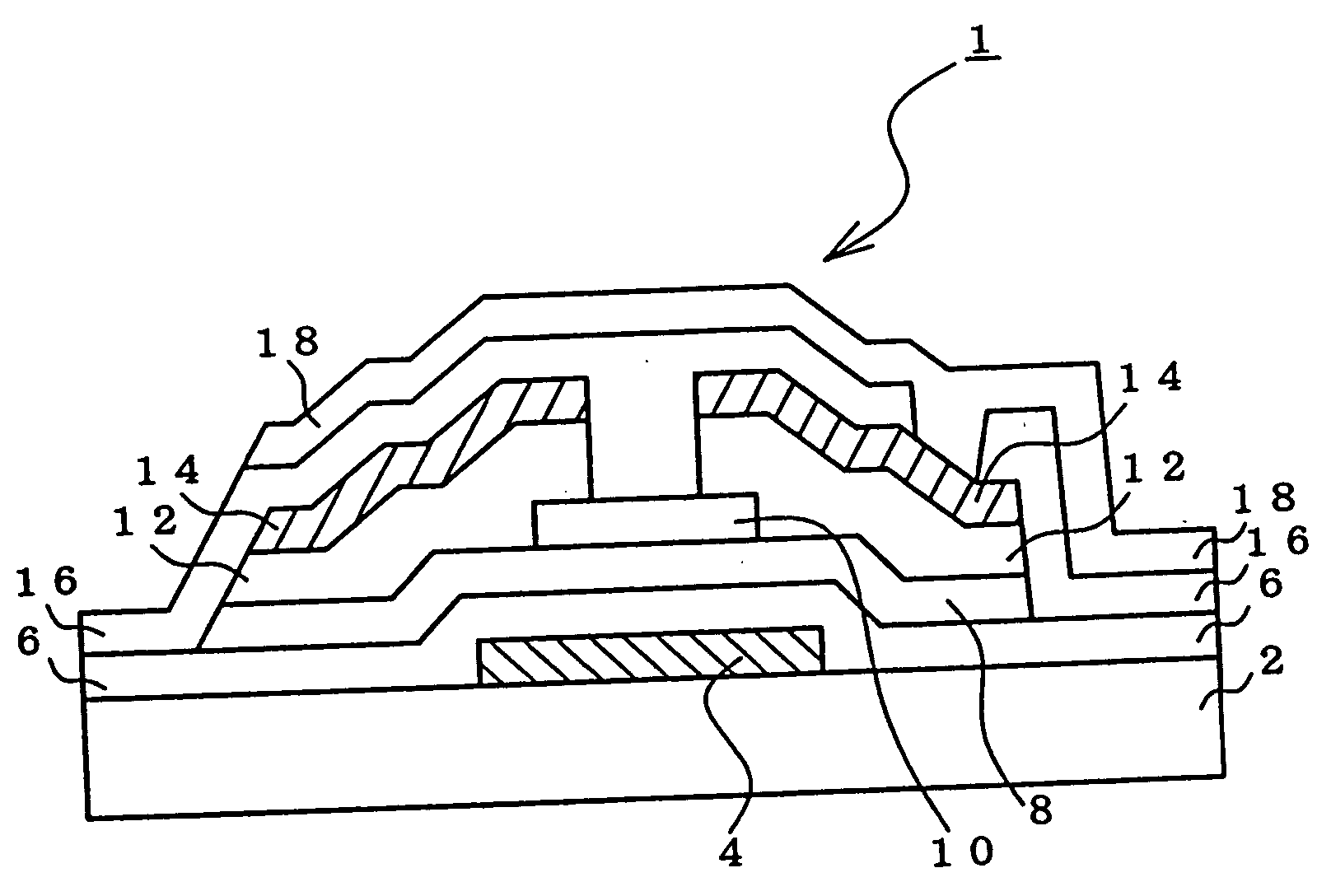
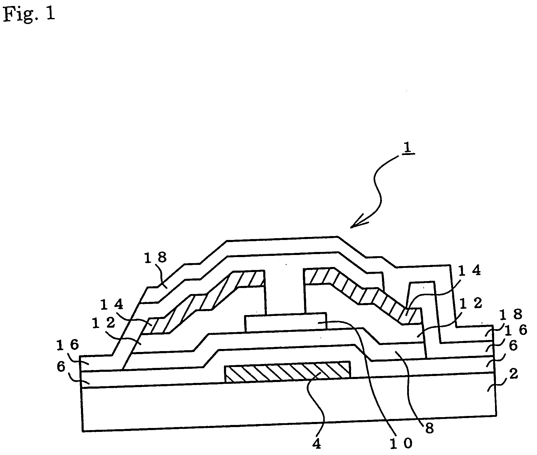
[0076] An embodiment of the invention will be described by using FIG. 1.

[0077] FIG. 1 is a cross sectional view showing an embodiment of a semiconductor device of the invention.

[0078] On a light transmittable glass substrate 2, a metal Ag (resistivity: 2.4 .mu..OMEGA..multidot.cm) containing 5% by weight of Mo was deposited to a film thickness of 2,500 .ANG. by high frequency sputtering. The layer was subjected to photoetching using a nitric acid-acetic acid-phosphoric acid solution as an etchant, thereby forming a gate electrode 4 (gate electrode wire) of a desired shape.

[0079] Next, a gate insulating film 6 as a first silicon nitride (SiNx) film (silicon layer) was deposited to a film thickness of 3,000 .ANG..

[0080] Subsequently, a SiH.sub.4--N.sub.2 mixed gas was used as a discharge gas and an .alpha.-Si:H(i) film (silicon layer) 8 was deposited to a film thickness of 3,500 .ANG..

[0081] Further, on the .alpha.-Si:H(i) film 8, by using an SiH.sub.4--NH.sub.3--N.sub.2 mixed gas as ...


PUM


Abstract

A semiconductor device 1 obtained by depositing, on a substrate 2, a gate electrode 4 formed by a conductive thin film containing Mo atoms and Ag atoms, a gate insulating film 6, an alpha-Si:H(i) film 8, a channel protection layer 10, an alpha-Si:H(n) film 12, a source/drain electrode 14 formed by a conductive thin film containing Mo atoms and Ag atoms, a source/drain insulating film 16, and a drive electrode 18. By using a conductive thin film containing Mo atoms and Ag atoms, the gate electrode 4 and the source/drain electrode 14 are formed to manufacture the semiconductor device 1. Thus, the conductive thin film for a semiconductor device, having high adhesion strength to a substrate, an insulating layer, and the like, a semiconductor device which operates stably without deteriorating the performance, and a method of efficiently manufacturing the conductive thin film and the semiconductor device can be provided.

Description

[0001] The present invention relates to a conductive thin film for a semiconductor device such as a semiconductor transistor, a semiconductor device, and a method of manufacturing the same.[0002] A TFT is a very important component as a main component of a display of a portable personal computer, a laptop personal computer, a television, or the like.[0003] Companies manufacture TFTs by their methods. Since the process of manufacturing a TFT is complicated and various metals and metal oxides are deposited a plurality of times, simplification of the process is demanded.[0004] In a process of manufacturing a conventional TFT array, as materials of a gate electrode and a source / drain electrode, metals such as Cr and TaW are used.[0005] Although Cr is easily processed, there is a problem that Cr is easily corroded. Although TaW is resistive to corrosion and the like, it has a problem of high electric resistance and the like.[0006] Consequently, a TFT array using wires made mainly of alum...

Claims


Application Information

Patent Timeline
IPC IPC(8): H01L21/285H01L21/288H01L21/336H01L29/45H01L29/49H01L29/786
CPCH01L21/2855H01L21/28568H01L21/32051H01L23/53247H01L29/458H01L2924/0002H01L29/4908H01L29/66765H01L2924/00H01L29/786
Inventor INOUE, KAZUYOSHIMATSUZAKI, SHIGEO
Owner IDEMITSU KOSAN CO LTD
Why Eureka
Try Eureka