Switching regulator having two or more outputs

a technology of switching regulators and outputs, applied in the direction of power conversion systems, instruments, dc-dc conversion, etc., can solve the problem that the size of particular industries is difficult to reduce, and achieve the effect of reducing excess consumption

Inactive Publication Date: 2005-05-31
SOCIONEXT INC
View PDF5 Cites 32 Cited by
  • Summary
  • Abstract
  • Description
  • Claims
  • Application Information

AI Technical Summary

Benefits of technology

[0024]In the switching regulator circuit described above, energy that would be conventionally converted into excess heat at the time of the stoppage of output power supply is returned to the DC power supply provided at the input end of the switching regulator. With this provision, excess consumption can be reduced through energy recharge if the DC power supply is a secondary buttery of a rechargeable type.

Problems solved by technology

Among various circuit components, an inductor in particular is difficult to reduce its size.

Method used


Image

  • Switching regulator having two or more outputs
  • Switching regulator having two or more outputs
  • Switching regulator having two or more outputs

Examples


first embodiment

[0047]FIG. 3 is a circuit diagram showing a switching regulator circuit according to the present invention.

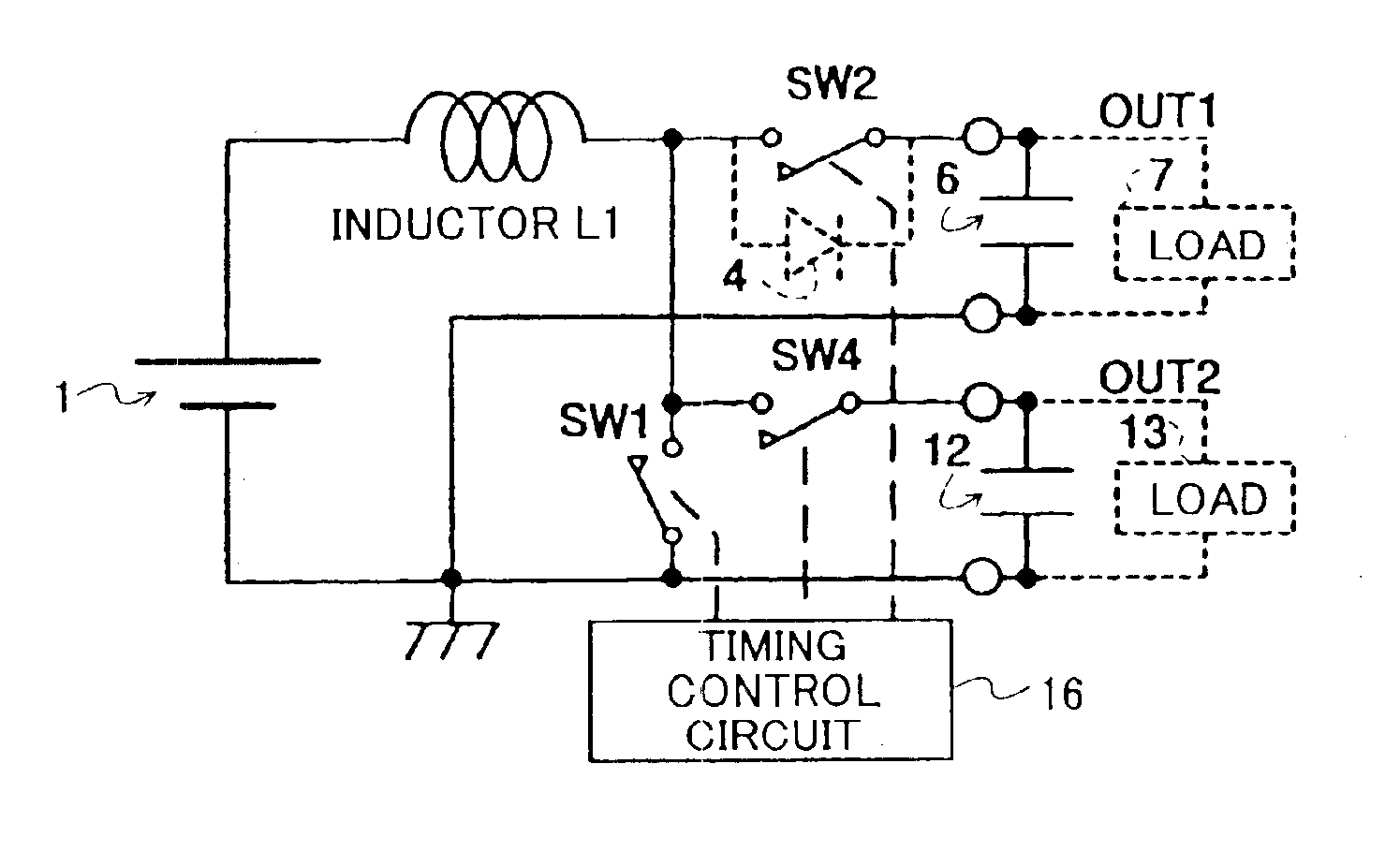
[0048]The switching regulator of FIG. 3 is coupled to a DC power supply 1, and includes an inductor L1 for shared use by OUT1 and OUT2, a semiconductor switch SW1 for providing a current to the inductor L1, a rectifying diode 4 for OUT1, a semiconductor switch SW2 for OUT1, a rectifying smoothing condenser 6 for OUT1, a semiconductor switch SW4 for OUT2, a rectifying smoothing condenser 12 for OUT2, and a timing control circuit 16. An output OUT1 appearing between the opposite ends of the rectifying smoothing condenser 6 is supplied to a load 7. An output OUT2 appearing between the opposite ends of the rectifying smoothing condenser 12 is supplied to a load 13.

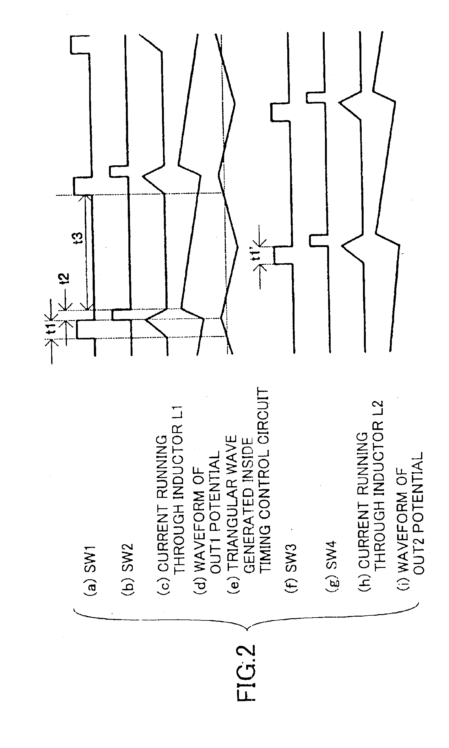
[0049]FIG. 4 is a timing chart for explaining the operation of the switching regulator shown in FIG. 3.

[0050]In FIG. 4, the switches SW1, SW2, and SW4 are closed (i.e., in a conductive state) during the HIGH period of res...

second embodiment

[0067]With the construction of the second embodiment as described above, the switch SW5 is closed at proper timing, so that residual energy in the inductor L1 remaining at the opening of the switch SW4 is prevented from leaking to the output OUT1 even when no load is connected to the output OUT1.

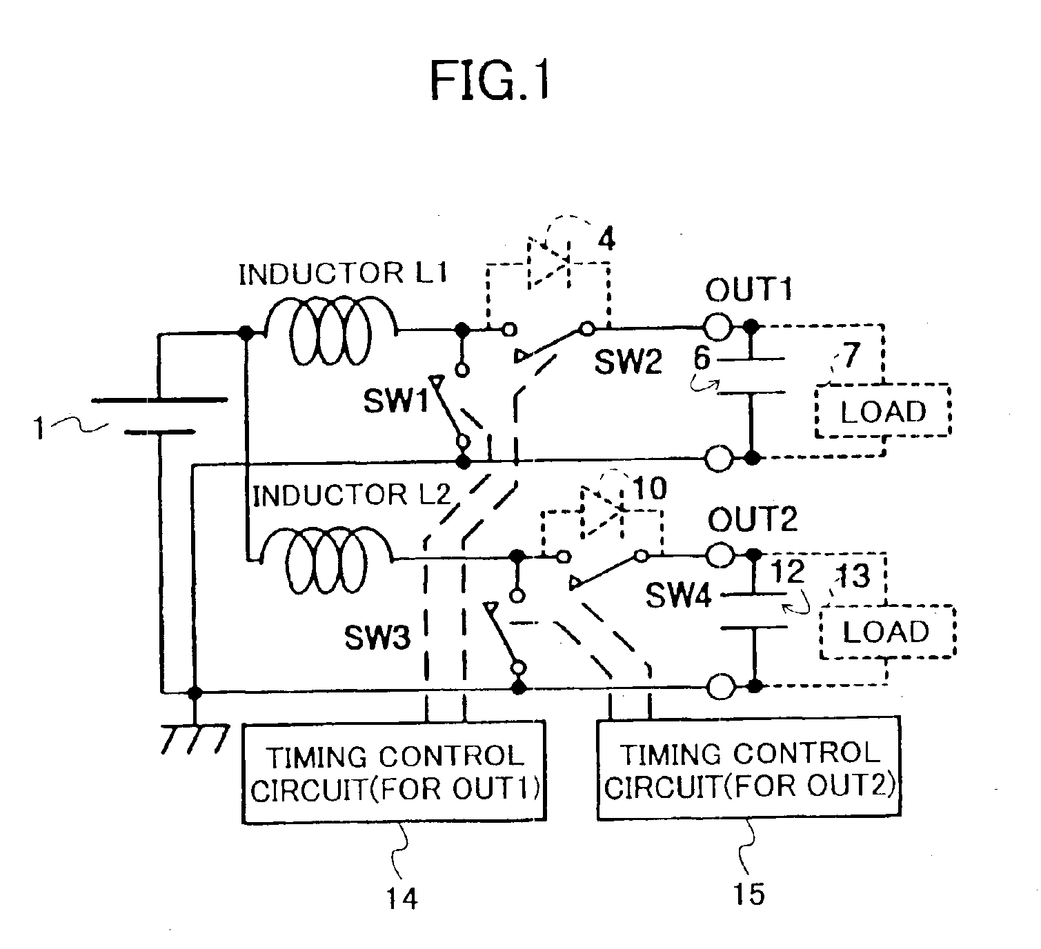
[0068]FIG. 7 is a circuit diagram showing a third embodiment of the switching regulator circuit according to the present invention. In FIG. 7, the same elements as those of FIG. 3 are referred to by the same numerals, and a description thereof will be omitted. The switching regulator of the third embodiment includes a diode series 22 replacing the diode 4 of the switching regulator of the first embodiment shown in FIG. 3. The diode series 22 is provided in parallel with the inductor L1.

[0069]In the construction shown in FIG. 7, the diode series 22 comprised of a plurality of diodes connected in series is provided in parallel with the inductor L1 for the purpose of preventing high potential f...

fourth embodiment

[0071]The fourth embodiment shown in FIG. 9 has the energy charging periods t1 and t5 different from each other where the periods t1 and t5 correspond to OUT1 and OUT2, respectively. When current consumption and output potential vary between the plurality of outputs OUT1 and OUT2, the periods t1 and t5 are independently controlled according to their needs. The maximum energy accumulated in the inductor L1 thus varies accordingly, thereby producing output potentials that match the required specifications.

[0072]In general, a timing control circuit for a switching regulator generates a triangular wave for controlling the switching timing. This triangular wave is shown in FIG. 2 and FIG. 4 as a timing reference. The potential of the triangular wave is compared with a predetermined threshold potential, thereby controlling the switching of each switch. In the fourth embodiment of FIG. 9, the positive transition time and the negative transition time of the triangular wave are controlled, s...


PUM


Abstract

A switching regulator circuit includes an inductor, a first condenser which provides a potential stored therein as a first output of the switching regulator circuit, a second condenser which provides a potential stored therein as a second output of the switching regulator circuit, and a switch set including a plurality of switches, the switch set establishing a first path, a second path, and a third path, the first path supplying energy from a DC power supply to the inductor for accumulation of the energy therein, the second path supplying the energy accumulated in the inductor to the first condenser, and the third path supplying the energy accumulated in the inductor to the second condenser.

Description

CROSS-REFERENCE TO RELATED APPLICATIONS[0001]The present application is based upon and claims the benefit of priority from prior Japanese Patent Application No. 2002-092767 filed on Mar. 28, 2002, with the Japanese Patent Office, the entire contents of which are incorporated herein by reference.BACKGROUND OF THE INVENTION[0002]1. Field of the Invention[0003]The present invention generally relates to switching regulators, and particularly relates to a switching regulator which supplies a plurality of DC power supply voltages.[0004]2. Description of the Related Art[0005]In recent years, switching regulators have been used in a variety of electrical equipment, resulting in a demand for a low-cost switching regulator occupying a small space.[0006]FIG. 1 is a circuit diagram showing a related-art switching regulator of a synchronous rectification type that can produce two output voltages higher than a input power potential.[0007]The switching regulator of FIG. 1 is coupled to a DC power ...

Claims


Application Information

Patent Timeline
Patent Type & Authority Patents(United States)
IPC IPC(8): H02M3/158H02M3/04H02M3/155
CPCH02M3/158H02M2001/009H02M1/009
Inventor NISHIMORI, EIJISEKIZAWA, TOSHIYUKI
Owner SOCIONEXT INC
Why Eureka
Try Eureka