Metal silicide forming method

A metal silicide and metal layer technology, which is applied in electrical components, semiconductor/solid-state device manufacturing, semiconductor devices, etc., can solve problems such as excessive metal diffusion and uneven thickness of metal silicide

Active Publication Date: 2020-03-17
CHANGXIN MEMORY TECH INC
View PDF11 Cites 0 Cited by
  • Summary
  • Abstract
  • Description
  • Claims
  • Application Information

AI Technical Summary

Problems solved by technology

[0005] The purpose of the present disclosure is to provide a method for forming metal silicide, and then at least to a certain extent overcom

Method used


Image

  • Metal silicide forming method
  • Metal silicide forming method
  • Metal silicide forming method

Examples


Embodiment Construction

[0026] Example embodiments will now be described more fully with reference to the accompanying drawings. Example embodiments may, however, be embodied in many forms and should not be construed as limited to the examples set forth herein; rather, these embodiments are provided so that this disclosure will be thorough and complete and will fully convey the concept of example embodiments to those skilled in the art. The described features, structures, or characteristics may be combined in any suitable manner in one or more embodiments.

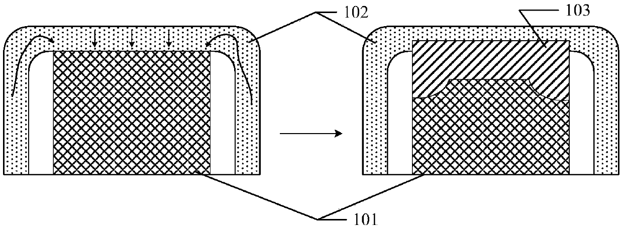
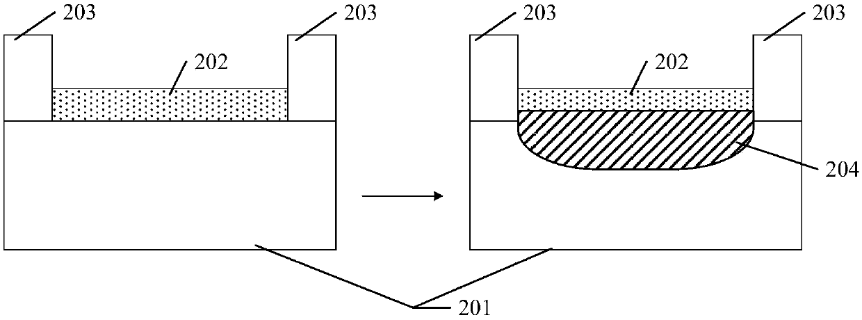
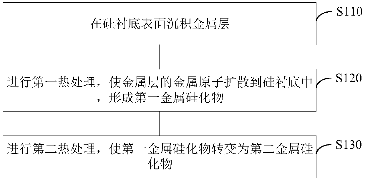
[0027] Exemplary embodiments of the present disclosure firstly provide a method for forming a metal silicide, referring to image 3 As shown, the method includes the following steps S110-S130:

[0028] Step S110, depositing a metal layer on the surface of the silicon substrate.

[0029] Step S120, performing a first heat treatment to diffuse metal atoms in the metal layer into the silicon substrate to form a first metal silicide.

[0030] Ste...


PUM


Abstract

The invention provides a metal silicide forming method, and belongs to the technical field of semiconductors. The method comprises the following steps: depositing a metal layer on the surface of a silicon substrate; performing first heat treatment to diffuse metal atoms of the metal layer into the silicon substrate to form a first metal silicide; carrying out second heat treatment to convert the first metal silicide into second metal silicide, wherein the temperature of the first heat treatment is lower than that of the second heat treatment. According to the invention, excessive diffusion ofmetal atoms in the forming process of the metal silicide can be reduced, the thickness uniformity of the metal silicide is improved, the performance of a semiconductor device is improved, and the service life of the semiconductor device is prolonged.

Description

technical field [0001] The present disclosure relates to the technical field of semiconductors, in particular to a method for forming a metal silicide. Background technique [0002] The information disclosed in this Background section is only for enhancement of understanding of the background of the disclosure and therefore it may contain information that does not form the prior art that is already known in the art to a person of ordinary skill in the art. [0003] In semiconductor manufacturing, metal silicides are usually formed by depositing metal atoms and diffusing. Most of the diffusion is achieved by rapid thermal processing (RTP) process, so that the metal atoms above the silicon substrate diffuse to the silicon substrate during rapid thermal processing. , the two react to form metal silicides. Contents of the invention [0004] In the existing metal silicide formation method, the rapid heat treatment generally adopts immersion annealing method (Soakanneal), becau...

Claims


Application Information

Patent Timeline
IPC IPC(8): H01L21/28H01L21/67
CPCH01L21/67248H01L21/28097
Inventor 不公告发明人
Owner CHANGXIN MEMORY TECH INC
Why Eureka
Try Eureka