Flexible membrane probe and method of use thereof

a flexible membrane and probe technology, applied in the direction of resistance/reactance/impedence, semiconductor/solid-state device testing/measurement, instruments, etc., can solve the problems of mercury posing a significant safety problem, time-consuming and costly metal or polysilicon contact fabrication, and unfitness of the entire semiconductor wafer for normal use, etc., to reduce the pressure of the fluid

Inactive Publication Date: 2005-05-31
SOLID STATE MEASUREMENTS
View PDF18 Cites 126 Cited by
  • Summary
  • Abstract
  • Description
  • Claims
  • Application Information

AI Technical Summary

Benefits of technology

[0019]The method can also include reducing the pressure of the fluid provided to the cavity sufficiently whereupo

Problems solved by technology

In other words, these contacts become permanent features on the semiconductor wafer, or the coating or film thereon, thereby making the entire semiconductor wafer unfit for normal use.
In addition, fabrication of the metal or polysilicon contacts is time-consuming and costly.
Problems may arise utilizing the Lederman mercury probe in that mercury may react chemically with the materials on the wafer under study.
Mercury can also pose a significant safety problem in its use under some conditions.
Thus, a mercury probe has limited application.
A problem with utilizing the probe disclosed in the Hillard patent for performing measurements is the need to grind the surface of the tip uniformly flat.
Another problem is the need to establis

Method used


Image

  • Flexible membrane probe and method of use thereof
  • Flexible membrane probe and method of use thereof
  • Flexible membrane probe and method of use thereof

Examples


Embodiment Construction

[0023]The present invention will be described with reference to the accompanying figures wherein like reference numbers correspond to like elements.

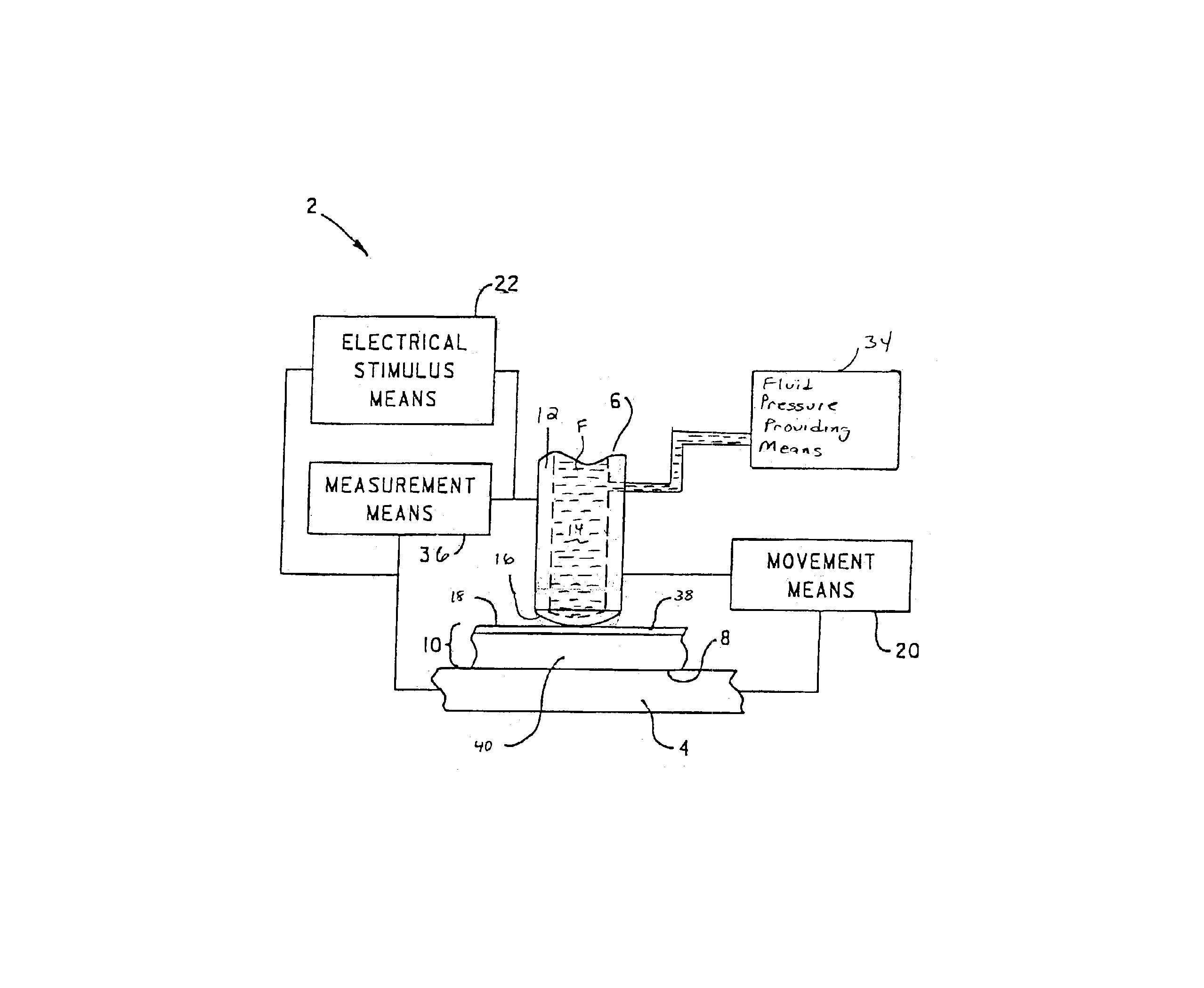
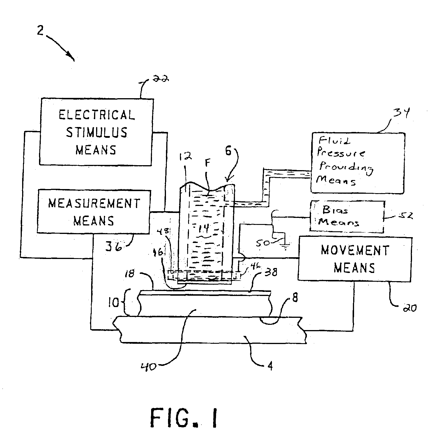
[0024]With reference to FIG. 1, a semiconductor wafer testing apparatus 2 includes an electrically conductive chuck 4 and a measurement probe 6. Chuck 4 is configured to support a backside 8 of a semiconductor wafer 10. Probe 6 has a probe body 12 defining a sealed internal cavity 14 that is in fluid communication with an electrically conductive and elastic or resilient membrane 16 affixed to a distal end of probe body 12. A movement means 20 can be connected to chuck 4, probe 6 or both for moving membrane 16 and a topside 18 of semiconductor wafer 10 into spaced relation.

[0025]An electrical stimulus means 22 is electrically connected between chuck 4 and membrane 16 for applying a suitable test stimulus to semiconductor wafer 10 when it is received on chuck 4 and membrane 16 is moved into contact with topside 18 of semiconductor wafer 10...


PUM


Abstract

A measuring apparatus for measuring a semiconductor wafer, or a film or coating thereon, includes an electrically conductive wafer chuck and a probe having a probe body defining an internal cavity in fluid communication with an electrically conductive and elastic or resilient membrane. The membrane and a topside of the semiconductor wafer are moved into spaced relation when the semiconductor wafer is supported by the wafer chuck. A pressure of fluid supplied to the internal cavity of the probe body is selectively controlled whereupon the membrane expands into contact with the topside of the semiconductor wafer. A suitable test stimulus is applied to the membrane and the semiconductor wafer and the response of the semiconductor wafer to the test stimulus is measured.

Description

BACKGROUND OF THE INVENTION[0001]1. Field of the Invention[0002]This invention relates to an apparatus and method for measuring electrical properties of a semiconductor wafer, or a coating or film on the semiconductor wafer.[0003]2. Description of Related Art[0004]The determination of electrical properties of a semiconductor wafer, or a coating or film thereon, is a critical factor in the production of such wafers. In current standard practice, measurements of these electrical properties have been accomplished by first fabricating one or more metal or doped polysilicon contacts on the top surface. These contacts become part of a metal oxide semiconductor (MOS) or Schottky barrier structure that is used to make the appropriate measurement. In other words, these contacts become permanent features on the semiconductor wafer, or the coating or film thereon, thereby making the entire semiconductor wafer unfit for normal use. Thus, these contacts are only formed on monitor or test semicon...

Claims


Application Information

Patent Timeline
IPC IPC(8): G01R1/073H01L21/66
CPCG01R1/0735
Inventor MAZUR, ROBERT G.
Owner SOLID STATE MEASUREMENTS
Why Eureka
Try Eureka