Transistor sidewall spacer stress modulation

a technology of sidewall spacers and transistors, which is applied in the direction of transistors, electrical devices, semiconductor devices, etc., can solve the problems of non-symmetric stress effects and affecting the performance of transistors, and achieve the effect of altering the stress effects of films

Inactive Publication Date: 2005-06-07
NORTH STAR INNOVATIONS
View PDF9 Cites 49 Cited by
  • Summary
  • Abstract
  • Description
  • Claims
  • Application Information

AI Technical Summary

Problems solved by technology

Unfortunately, some of the more prevalent spacer materials tend to impact the transistor's performance.
Even worse, these stress effects tend to be non-symmetrical with respect to n-channel and p-channel transistors in a CMOS process.

Method used


Image

  • Transistor sidewall spacer stress modulation
  • Transistor sidewall spacer stress modulation
  • Transistor sidewall spacer stress modulation

Examples


Embodiment Construction

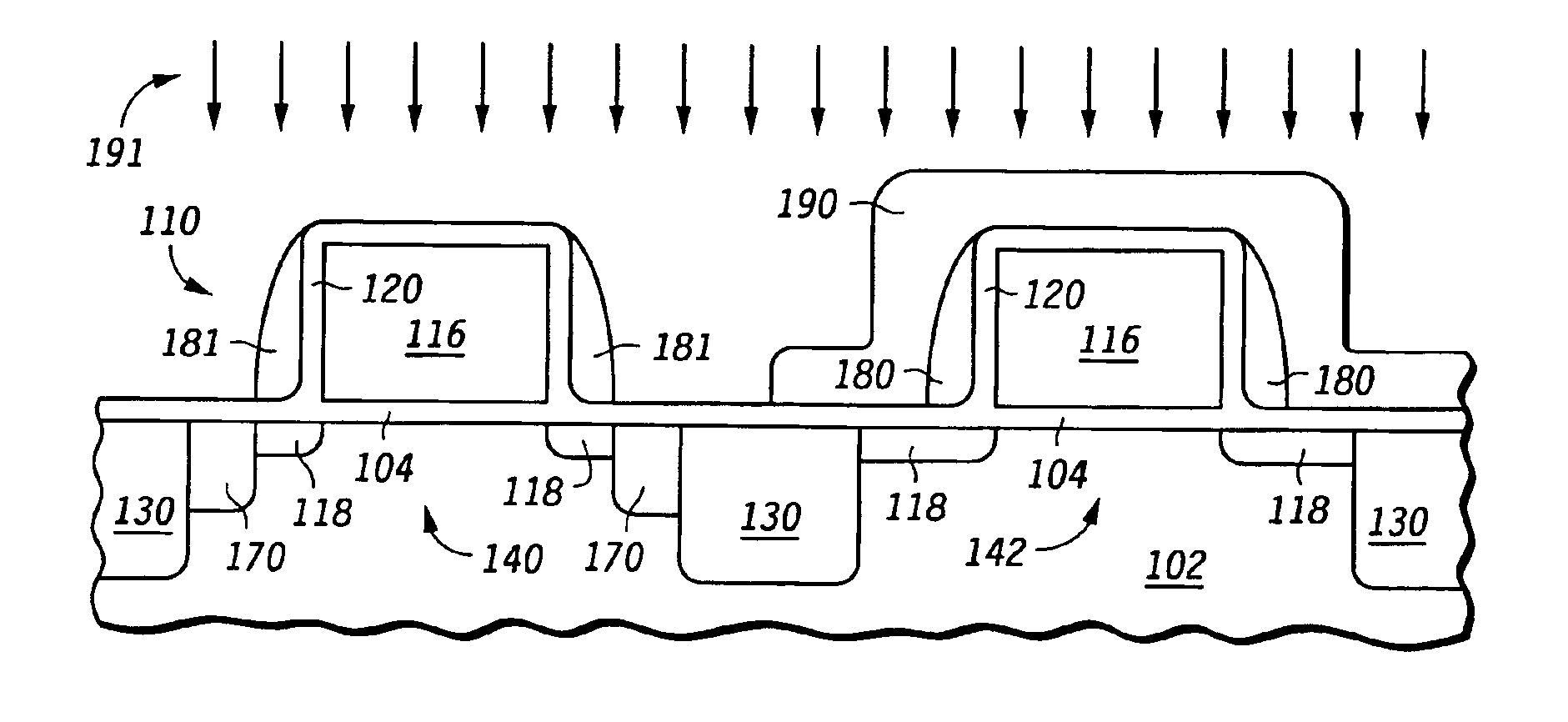
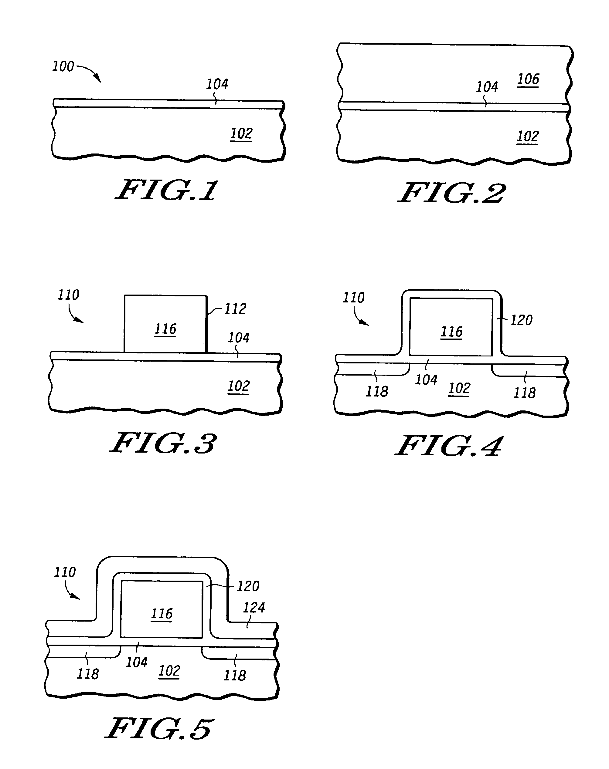
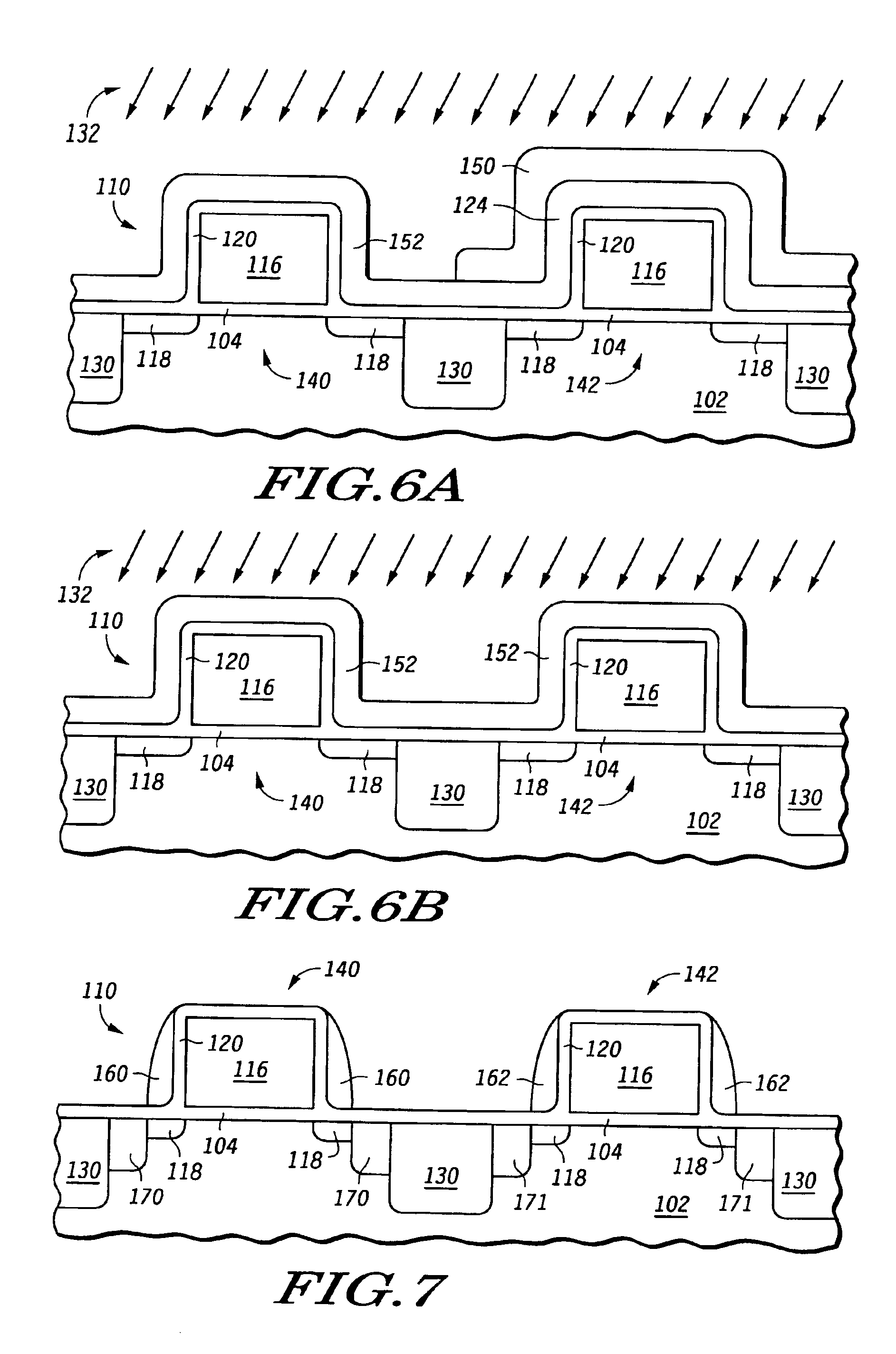
[0019]Reference will now be made in detail in the presently preferred embodiments of the invention, examples of which are illustrated in the accompanying drawings. It should be noted that the drawings are in simplified form and are not to precise scale. Although the invention herein refers to certain illustrated embodiments, it is to be understood that these embodiments are presented by way of example and not by way of limitation. The intent of the following detailed description is to cover all modifications, alternatives, and equivalents as may fall within the spirit and scope of the invention as defined by the appended claims.

[0020]It is to be understood and appreciated that the process steps and structures described herein do not cover a complete process flow for the manufacture of an integrated circuit. The present invention may be practiced in conjunction with various integrated circuit fabrication techniques that are conventionally used in the art, and only so much of the comm...


PUM


Abstract

A semiconductor fabrication process and the resulting integrated circuit include forming a gate electrode (116) over a gate dielectric (104) over a semiconductor substrate (102). A spacer film (124) exhibiting a tensile stress characteristic is deposited over the gate electrode (116). The stress characteristics of at least a portion of the spacer film is then modulated (132, 192) and the spacer film (124) is etched to form sidewall spacers (160, 162) on the gate electrode sidewalls. The spacer film (124) is an LPCVD silicon nitride in one embodiment. Modulating (132) the spacer film (124) includes implanting Xenon or Germanium into the spacers (160) at an implant energy sufficient to break at least some of the silicon nitride bonds. The modulation implant (132) may be performed selectively or non-selectively either before or after etching the spacer film (124).

Description

BACKGROUND OF THE INVENTION[0001]1. Field of the Invention[0002]The present invention relates generally to the field of semiconductor fabrication and, more particularly, to a process of fabricating transistors having sidewall spacers.[0003]2. Description of Related Art[0004]The use of sidewall spacers in the formation of metal-oxide-semiconductor (MOS) transistors is well known. A spacer is a structure located adjacent to the sidewalls of a transistor's gate. After forming the transistor gates, the spacers are typically formed by following a conformal deposition process with an anisotropic etch. Portions of the deposited film adjacent vertically oriented portions of the pre-deposition topography remain after the etch. Sidewall spacers provide an implant block that enables, for example, lateral displacement of heavily doped source / drain regions from the edges of the transistor gate. This displacement is beneficial in reducing short channel effects of submicrons and deep submicron tra...

Claims


Application Information

Patent Timeline
Patent Type & Authority Patents(United States)
IPC IPC(8): H01L21/265H01L21/336H01L21/02H01L29/78H01L21/70H01L29/66H01L21/8234
CPCH01L21/26586H01L21/823468H01L29/7842H01L29/6659H01L29/7833H01L29/6656
Inventor GRUDOWSKI, PAUL A.
Owner NORTH STAR INNOVATIONS
Why Eureka
Try Eureka