Semiconductor device, liquid crystal module adopting same, method of manufacturing liquid crystal module, and electronic equipment adopting same

a technology of liquid crystal modules and semiconductors, applied in the direction of optical elements, identification means, instruments, etc., can solve the problem of difficulty in realizing a compact size structure for an increased number of pixels, and achieve the effect of reducing the module structure and thin structur

Inactive Publication Date: 2005-06-07
SHARP KK
View PDF15 Cites 41 Cited by
  • Summary
  • Abstract
  • Description
  • Claims
  • Application Information

AI Technical Summary

Benefits of technology

[0024]Therefore, as will be described later, in its application to a liquid crystal module wherein the semiconductor device and the liquid crystal panel are provided so as to face one another, it is possible to connect the external connection terminals of the flexible substrate to the inner surface of a module main body in the state where the semiconductor element of the semiconductor device is provided so as to face the inside of the module main body. As a result, it is possible to mount a semiconductor element without adopting such undesirable arrangement that the semiconductor element is projected to the outside of the liquid crystal module main body can be avoided. It is therefore possible to reduce the module structure by the thickness of the semiconductor element, thereby permitting a liquid crystal module of a thinner structure.
[0025]Additionally, for example, in a liquid crystal module wherein the semiconductor device, the liquid crystal panel, and the printed wiring substrate are mounted in flat, a semiconductor element can be mounted without adopting such undesirable arrangement that the semiconductor element is provided between the liquid crystal panel and the printed wiring substrate can be avoided.
[0026]As a result, the semiconductor device which realizes a device adopting the same of a thinner or shorter structure can be provided.

Problems solved by technology

For this reason, it is difficult to realize a compact size structure for an increased number of pixels.
However, in the conventional semiconductor device and the liquid crystal module adopting the conventional semiconductor device have the following problems.

Method used


Image

  • Semiconductor device, liquid crystal module adopting same, method of manufacturing liquid crystal module, and electronic equipment adopting same
  • Semiconductor device, liquid crystal module adopting same, method of manufacturing liquid crystal module, and electronic equipment adopting same
  • Semiconductor device, liquid crystal module adopting same, method of manufacturing liquid crystal module, and electronic equipment adopting same

Examples


first embodiment

[First Embodiment]

[0040]The following descriptions will explain one embodiment of the present invention with reference to FIGS. 1 through 3(b). A liquid crystal module in accordance with the present invention is applicable to, for example, a small-size electronic equipment such as a portable phone, pager, a game machine, etc.

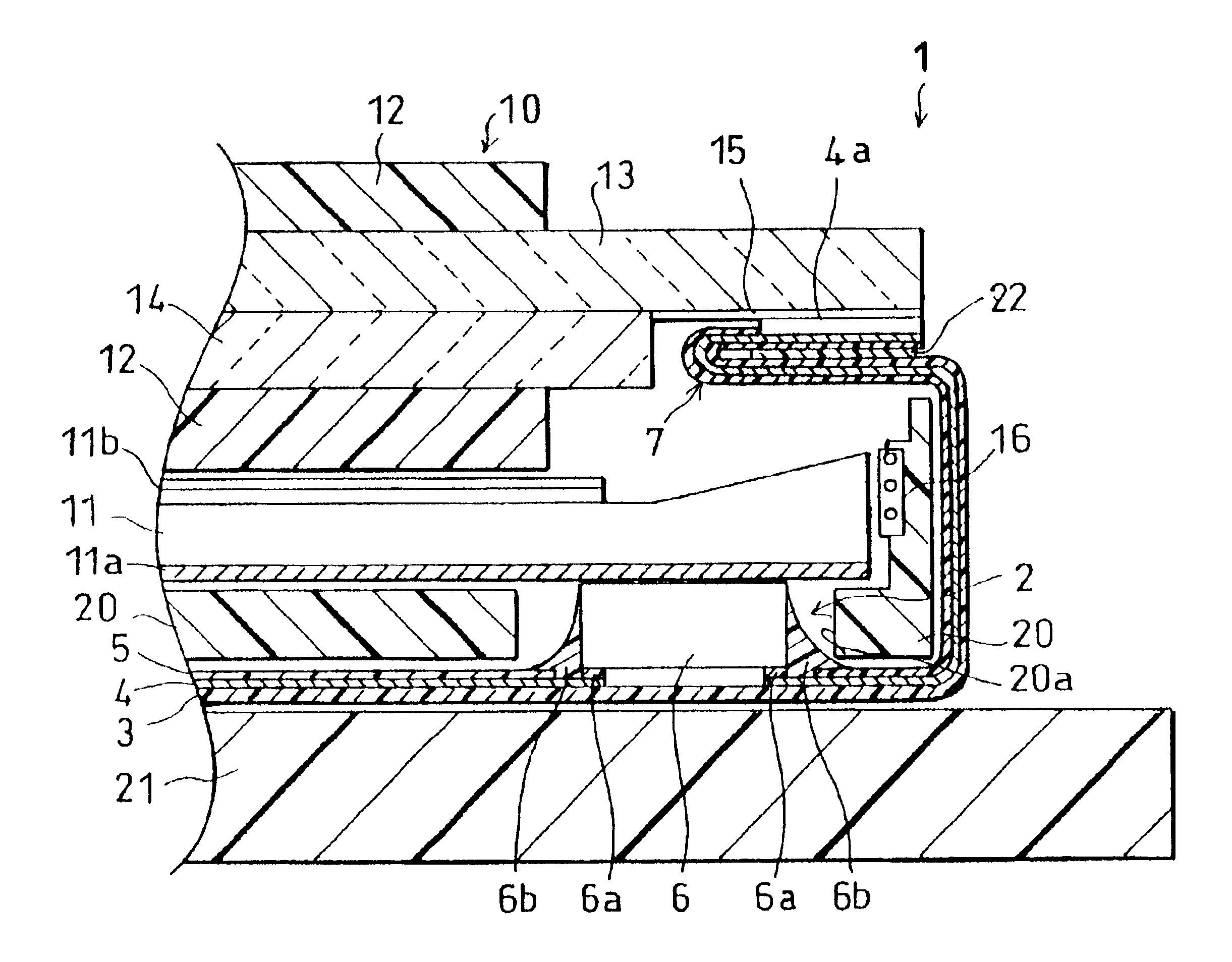
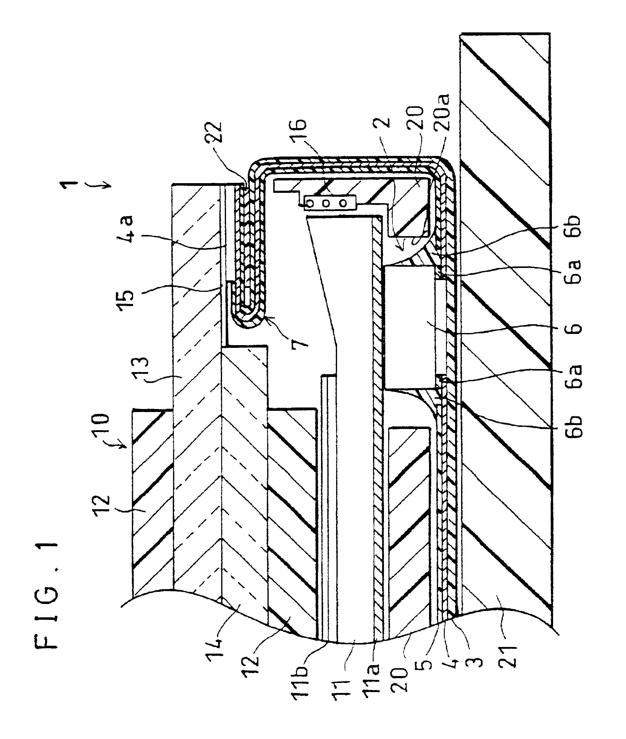
[0041]As illustrated in FIG. 1, a liquid crystal module 1 in accordance with the present embodiment includes a light-directing plate 11 (lighting means) formed above a frame 20 via a reflective sheet 11a. Further, above the light-directing plate 11, formed via a diffusing plate 11b is a liquid crystal panel 10 (member to be connected) comprised of an upper glass substrate 13 and a lower glass substrate 14 interposed between polarization plates 12. Between the upper glass substrate 13 and the lower glass substrate 14, a liquid crystal layer (not shown) and an electrode 15 are interposed. The upper glass substrate 13 is formed longer than the lower glass substrate...

second embodiment

[Second Embodiment]

[0073]The following will explain still another embodiment of the present invention in reference to FIGS. 4 through 5(b). For ease of explanation, members (structures) having the same functions as those shown in the drawings pertaining to the first embodiment above will be given the same reference symbols, and explanation thereof will be omitted here. It should be noted here that respective characteristic structures of the first embodiment are applicable to the present embodiment.

[0074]As illustrated in FIG. 4, the liquid crystal module 30 in accordance with the present embodiment is arranged such that the semiconductor device 2 is connected to the liquid crystal panel 40 (member to be connected) in flat.

[0075]Specifically, the liquid crystal panel 40 of the liquid crystal module 30 is composed of an upper glass substrate 42 and a lower glass substrate 43 interposed between polarization plates 41. Further, between the upper glass substrate 42 and the lower glass su...

third embodiment

[Third Embodiment]

[0093]The following will explain still another embodiment of the present invention in reference to FIGS. 6(a) through 8(c). For ease of explanation, members (structures) having the same functions as those shown in the drawings pertaining to the first embodiment will be given the same reference symbols, and explanation thereof will be omitted here. It should be noted here that respective characteristic structures of the first embodiment are applicable to the present embodiment.

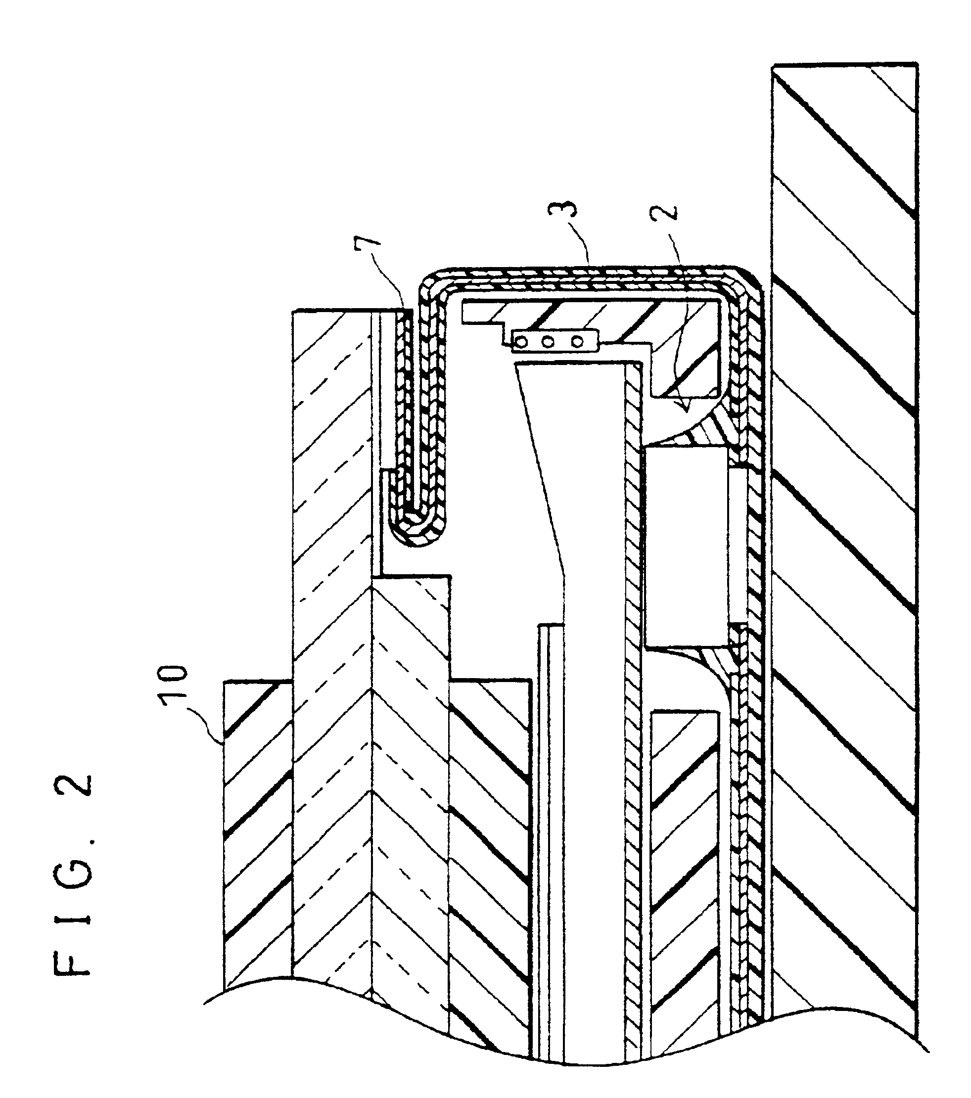
[0094]In the present embodiment and also in the next fourth embodiment, in the manufacturing method of the liquid crystal modules 1 and 30, the method of forming U-shaped folded part 7 of the semiconductor device 2 adopted in the first and second embodiments and the method of connecting the liquid crystal panels 10 and 40 will be explained. In the present embodiment, explanations will be given through the case wherein the U-shaped folded part 7 of the semiconductor device 2 is connected to the...


PUM

PropertyMeasurementUnit
thicknessaaaaaaaaaa
flexibleaaaaaaaaaa
semiconductoraaaaaaaaaa

Abstract

A semiconductor device of the present invention includes a film-like flexible substrate having formed thereon a wiring pattern, external connection terminals formed at both end portions of the flexible substrate; and a semiconductor element mounted on a surface side of the flexible substrate, wherein a folded part, which is folded down in U-shape to a back surface side of the flexible substrate, is formed in a fixed state at least at one end portion of the flexible substrate. With this structure, the semiconductor device is COF mounted, and, for example, in its application to a liquid crystal module wherein the semiconductor device is provided so as to face a liquid crystal panel, the external connection terminals of the flexible substrate can be connected to an inner surface of a module main body for a liquid crystal panel in a state the semiconductor element of the semiconductor device faces the inside of the module main body. As a result, since the semiconductor element can be mounted without being projected to the outside of the module main body, the liquid crystal module can be made thinner for the thickness of the semiconductor element.

Description

FIELD OF THE INVENTION[0001]The present invention relates to a so-called COF (Chip-On-Film) type semiconductor device wherein a semiconductor element is mounted on a flexible wiring substrate, a liquid crystal module wherein a liquid crystal panel is connected to the semiconductor device and a method of manufacturing the liquid crystal module, and an electric component adopting the liquid crystal module, and more particularly relates to a connection structure of external connection terminals of the semiconductor device. The liquid crystal module is applicable to, for example, a portable phone, an automobile navigation equipment system, a personal data assistant (PDA), a word processor, a personal computer, television sets, motors, etc.BACKGROUND OF THE INVENTION[0002]A semiconductor device of a so-called COF (Chip-On-Film) structure wherein a semiconductor element is joined to or mounted on a flexible wiring substrate has been used in a variety of fields, and hereinafter, the semico...

Claims


Application Information

Patent Timeline
Patent Type & Authority Patents(United States)
IPC IPC(8): G02F1/13H05K3/36G02F1/1345G02F1/1333G09F9/00H05K1/11H05K1/14
CPCG02F1/13452H05K3/361G02B6/0083H05K2201/055G02F1/133615G02B6/0073H05K2201/10681H01L2224/16225H01L2224/32225H01L2224/73204H01L2924/00014H01L2924/00H01L2224/0401G02F1/1333
Inventor FUKUTA, KAZUHIKOIWANE, TOMOHIKOMONZEN, MASAHIKO
Owner SHARP KK
Why Eureka
Try Eureka