Imager cell with pinned transfer gate

a transfer gate and imager technology, applied in the field of cmos imager cells, can solve the problems of undesired image alteration during integration and readout, high read noise, prior photoreceptor cells were not tailored to provide adequate response over a wide range of light levels, etc., to achieve enhanced blue light response and low noise

Inactive Publication Date: 2005-06-21
ESS TECH INT INC +1
View PDF6 Cites 18 Cited by
  • Summary
  • Abstract
  • Description
  • Claims
  • Application Information

AI Technical Summary

Benefits of technology

[0010]An improved imager cell is arrived at by incorporating a “pinned transfer gate” between a photoreceptor and a sense node. The imager cell may be broadly conceptualized as a light detecting element with

Problems solved by technology

However, passive photoreceptor cells, while having high quantum efficiency, were plagued with high read noise.
Furthermore, the n+ contacts used in active photoreceptor cells generated significant dark current, there

Method used


Image

  • Imager cell with pinned transfer gate
  • Imager cell with pinned transfer gate
  • Imager cell with pinned transfer gate

Examples


Embodiment Construction

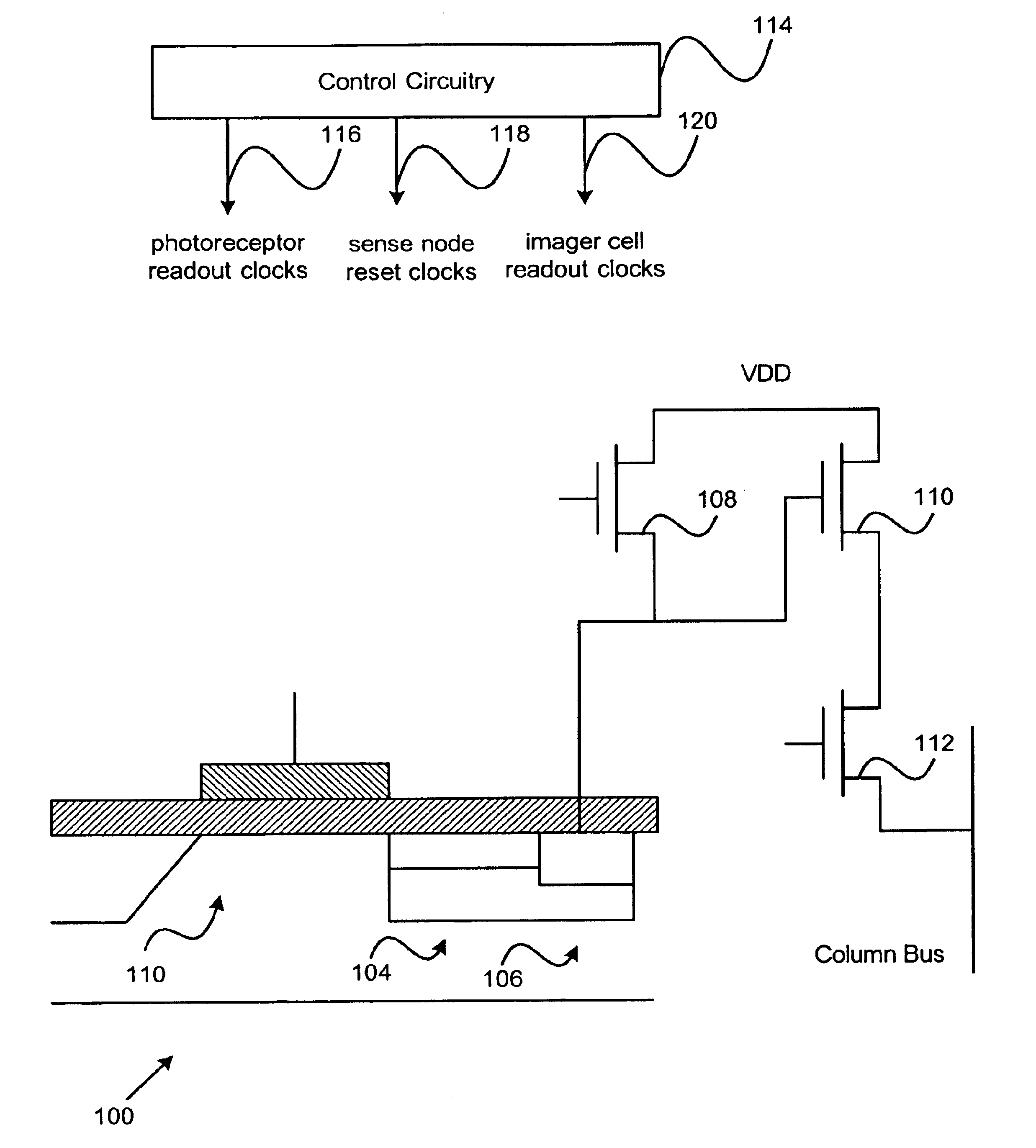
[0027]With regard first to FIG. 1, an imager cell 100 (descried in more detail below) includes a photoreceptor 102, a transfer gate 104, and a sense node 106. A reset transistor 108 is provided to reset the sense node 106, and an output amplifier 110 provides sense node buffering when the sense node 106 is readout to the column bus through the select transistor 112. Also illustrated in FIG. 1 is control circuitry 114 that produces photoreceptor readout clocks 116, sense node reset clocks 118, and imager cell readout clocks 120. The control circuitry 114 may generally be implemented as a conventional CMOS imager controller, except with regard to the operating modes described in more detail below and with regard to the applicable integration voltages that setup preselected charge capacity levels in the photoreceptor 102.

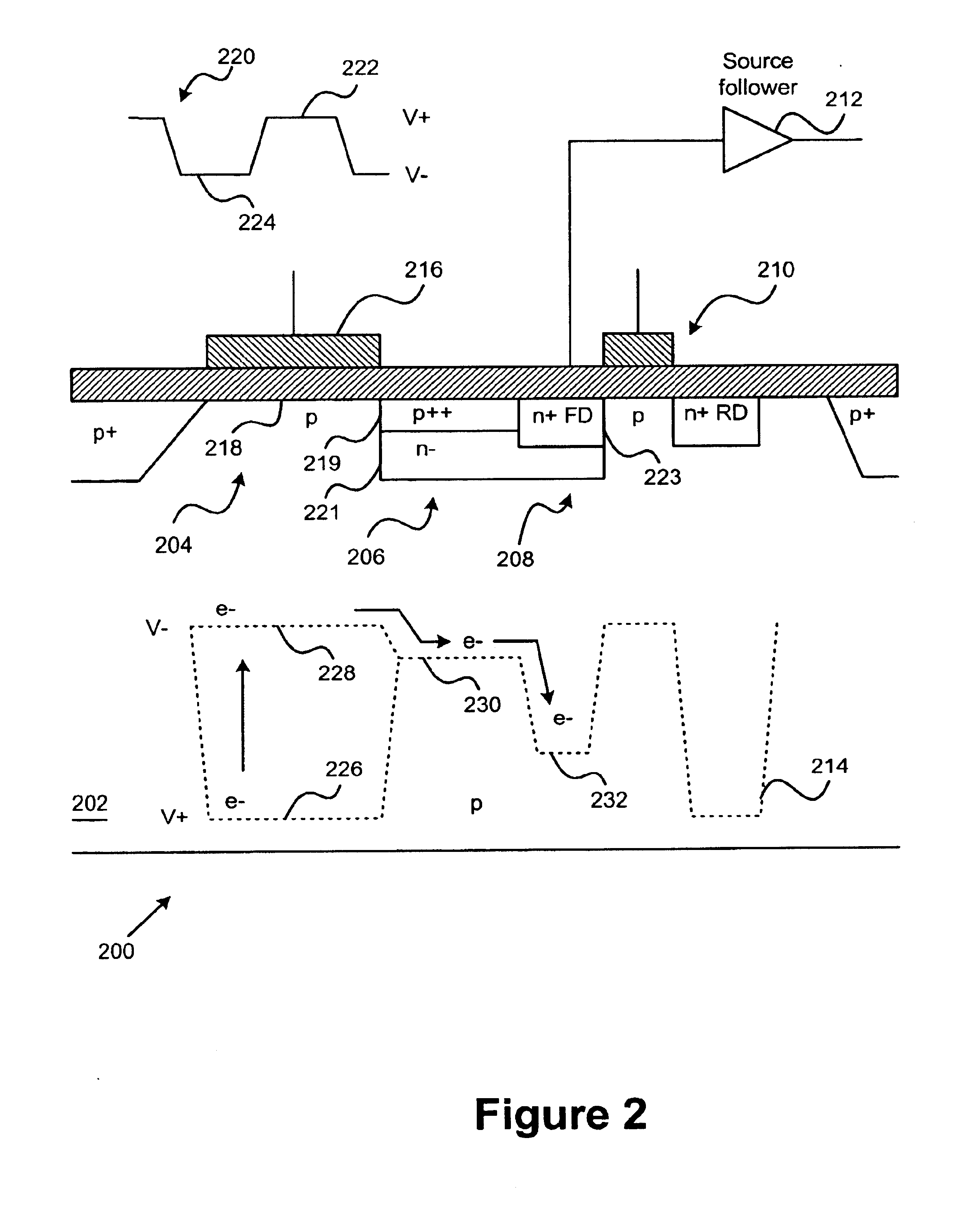
[0028]Turning next to FIG. 2, that figure presents a more detailed view of an imager cell 200. The imager cell 200 is formed in a p-type substrate 202 and includes a p...


PUM


Abstract

An imager cell includes a photoreceptor, a sense node, and a pinned transfer gate. The pinned transfer gate is tied to the same potential of a substrate of the imager cell and is disposed between the photoreceptor and the sense node in order to transfer charge between the photoreceptor and the sense node. The imager further includes a reset transistor disposed to reset the sense node, and an output amplifier coupled to the sense node. Control circuitry supplies a photoreceptor readout clock to the photoreceptor. The readout clock includes an integration period and a transfer period. According to various embodiments of the invention, the imager cell provides improved noise performance, selective charge capacities, and improved blue light response beyond that of conventional imager cells.

Description

RELATED APPLICATION DATA[0001]This continuation-in-part application claims priority to U.S. patent application Ser. No. 09 / 977,444 filed on Oct. 15, 2001, now U.S. Pat. No. 6,762,441, which application is incorporated by reference to the extent permitted by law.BACKGROUND OF THE INVENTION[0002]1. Field of the Invention[0003]This invention relates to electronic imaging devices, and in particular to a CMOS imager cell incorporating a “pinned transfer gate”.[0004]2. Related Art[0005]Electronic imaging devices (“imagers”) find use in a broad range of applications in many distinct fields of technology including the consumer, industrial, medical, defense and scientific fields. Imagers use an array of photoreceptors to convert photons bearing image information into electrical signals representative of the image.[0006]In recent years, CMOS imagers have become a practical implementation option and provide cost and power advantages over other technologies such as charge coupled devices (CCD)....

Claims


Application Information

Patent Timeline
IPC IPC(8): H01L29/78H01L29/66H01L27/146
CPCH01L27/14645H01L27/14609
Inventor JANESICK, JIM
Owner ESS TECH INT INC
Why Eureka
Try Eureka