
Semiconductor device with dummy structure

a technology of dummy regions and semiconductors, applied in semiconductor devices, semiconductor/solid-state device details, electrical equipment, etc., can solve the problems of adverse effects of lithography process for upper layer, other problems of forming dummy regions, etc., and achieve the effect of preventing electric shortage between wells

Active Publication Date: 2005-06-21
FUJITSU SEMICON LTD
View PDF4 Cites 14 Cited by
  • Summary
  • Abstract
  • Description
  • Claims
  • Application Information

AI Technical Summary

Benefits of technology

[0024]An object of this invention is to provide a semiconductor device capable of ensuring surface flatness by using dummies and suppressing the influence of dummies upon the device.
[0025]Another object of the invention is to provide a semiconductor device capable of making uniform parasitic capacitances of an upper level wiring layer even if dummies are formed, and capable of preventing electric shortage between wells even if a silicide process is incorporated.
[0027]Even if dummy structures are formed, electric malfunction such as electric shortage between wells can be prevented. Parasitic capacitances of a wiring layer formed above dummy structures can be made uniform.

Problems solved by technology

In an active region having a small width sandwiched between trench portions having a large width or in a region where active regions having a small width are dense, CMP does not stop at the silicon nitride film and the active regions are polished, resulting in erosion.
If the flatness of the substrate surface is lost because of such phenomena, a later lithography process for an upper layer is adversely affected.
However, forming dummy regions may pose other problems.
This problem occurs when the active region dummy and local interconnect dummy are designed independently.

Method used


Image

  • Semiconductor device with dummy structure
  • Semiconductor device with dummy structure
  • Semiconductor device with dummy structure

Examples


Embodiment Construction

[0035]Embodiments of the invention will be described with reference to the accompanying drawings.

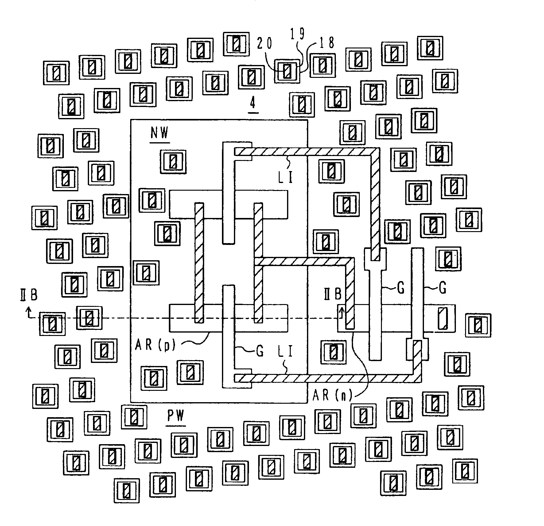
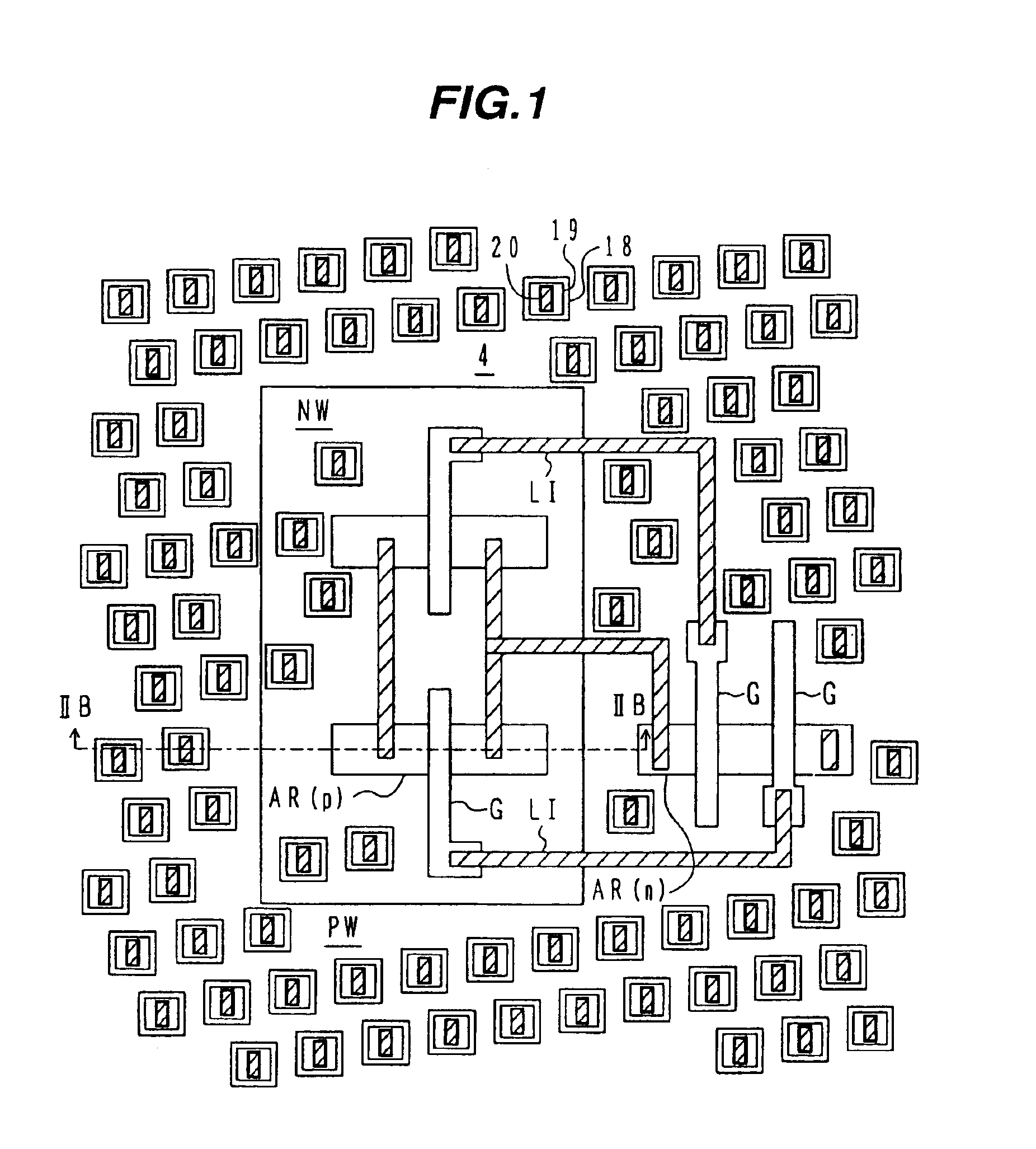
[0036]FIG. 1 shows a plan layout of a semiconductor device according to an embodiment of the invention. Active regions AR(n) and AR(p) are defined by an isolation region 4 formed by STI. The active region AR(p) for a p-channel MOS transistor is disposed in an n-type well NW. A p-type well PW is disposed surrounding the n-type well NW. The active region AR(n) for an n-channel MOS transistor is disposed in the p-type well PW. Active region dummies 18 are disposed in the n-type well NW and p-type well PW in such a manner that they will not lie across the boundary between the n-type well NW and p-type well PW.

[0037]Gate electrodes G are formed traversing the active region AR(n). A gate electrode dummy 19 is formed on each active region dummy 18 by using the same layer as that of the gate electrode G. Local interconnects LI are formed interconnecting desired regions of semiconductor elements ...


PUM


Abstract

A semiconductor device having: a semiconductor substrate with an isolation region defining a plurality of active regions; a gate electrode formed above each active region, constituting a semiconductor element; an interlevel insulator covering the gate electrode; local interconnects formed through the interlevel insulator and electrically connected to the semiconductor element; local interconnect dummies formed through the interlevel insulator and electrically separated from the local interconnects; and lower level dummies, each comprising either one of an active region dummy, a laminated dummy of an active region dummy and a gate electrode dummy formed thereon, and a gate electrode dummy formed on the isolation region, wherein each of the local interconnect dummies is not connected to two or more lower level dummies.

Description

CROSS REFERENCE TO RELATED APPLICATION[0001]This application is based on and claims priority of Japanese Patent Application No. 2002-317758 filed on Oct. 31, 2002, the entire contents of which are incorporated herein by reference.BACKGROUND OF THE INVENTION[0002]A) Field of the Invention[0003]The present invention relates to a semiconductor device, and more particularly to a semiconductor device having a dummy structure which does not function as part of an electronic circuit. The dummy structure is made of an active region dummy, a gate electrode dummy, a local interconnect dummy or the like.[0004]B) Description of the Related Art[0005]Since the recent integration degree of semiconductor integrated circuit devices is high, shallow trench isolation (STI) excellent in planarization has been adopted as isolation techniques in place of local oxidation of silicon (LOCOS). Since the gate length is becoming shorter than ever, a high patterning precision is required to form a gate electrod...

Claims


Application Information

Patent Timeline
IPC IPC(8): H01L23/52H01L23/522H01L21/02H01L21/3105H01L21/76H01L21/3205H01L21/762H01L21/768H01L21/82H01L21/822H01L21/8234H01L27/02H01L27/04H01L27/08H01L27/088
CPCH01L21/76229H01L21/7684H01L21/76895H01L21/823437H01L21/823475H01L27/0207H01L21/31053H01L2924/0002H01L23/522H01L2924/00H01L21/82
Inventor NANJO, RYOTA
Owner FUJITSU SEMICON LTD
Learn More