Method of erasing repeated patterns and pattern defect inspection device

a pattern defect and repeating pattern technology, applied in image enhancement, instruments, image data processing, etc., can solve the problems of poor throughput, time-consuming and laborious, and difficulty in identifying the precise position of defects,

Inactive Publication Date: 2005-06-21
PANASONIC CORP
View PDF7 Cites 33 Cited by
  • Summary
  • Abstract
  • Description
  • Claims
  • Application Information

AI Technical Summary

Benefits of technology

[0023]An object of the present invention is to solve the above problems and to provide a method of erasing repeated patterns in which inspection of defects in a repeated pattern can be performed without problems.
[0024]A method of erasing repeated patterns according to the present invention comprises, in a dark / light image obtained by image pickup of a subject of inspection, when identifying defects present in a repeated pattern in a subject of inspection, a step of detecting a plurality of density differences in which the density differences are found between reference pixels separated by values of a predetermined reference size and sizes which are integral multiples thereof and a plurality of comparison pixels, a step of determining a specific density difference wherein the density difference that is closest to 0 or the mean density difference from a plurality of density differences is detected as specific density difference, and a pattern-erased image generation step in which the specific density difference is applied to the reference density in the pattern-erasure image; by detecting the specific density differences using the density differences with respect to a plurality of comparison pixels, the problems mentioned above are eliminated and a repeated pattern can be suitably erased without using a complicated algorithm.
[0025]Also, a pattern defect inspection device according to the present invention comprises an image pickup element that picks up an image of an inspection subject and a processing device that detects pattern defects by storing and processing dark / light image data obtained by image pickup of the inspection subject wherein the processing device comprises: a portion for detecting a plurality of density differences in which the density differences are found between reference pixels separated by a pre-determined reference size and sizes which are integral multiples thereof and a plurality of comparison pixels; a specific density difference determining portion wherein the density difference that is closest to 0 from a plurality of density differences is detected, a pattern-erased image generation portion in which the specific density difference is applied to the reference density in the pattern-erasure image; and a defect detection portion; thus the repeated pattern can be erased and pattern defects detected in a suitable way as described above.

Problems solved by technology

In the case of visual inspection, alterations in the type of electronic equipment being inspected can easily be coped with, and start-up is rapid, but there are the drawbacks that identifying the precise positions of defects takes time and throughput is poor.
Maintaining and standardizing detection sensitivity is also a problem.
In contrast, in the case of image processing using a machine, although there are the advantages that rapid identification of the precise positions of defects and maintenance and standardization of the detection sensitivity can be achieved, there was the problem that considerable time was required for adjustment in the event of alterations in the type of electronic equipment being manufactured.
With increases in the structural fineness and performance of components in recent years, the poor throughput of visual inspection has become increasingly prominent.
However, although the structural fineness and performance of electronic equipment devices such as liquid crystal panels, plasma or display panels and semiconductor wafers has considerably increased, these devices are often formed with a large number of repeated patterns identical to a partial pattern.
Secondly, pixels whose density differs considerably from the background density of the background image are detected as defects.
Firstly, normal portions of the pattern are left in the background image.
Secondly, although they might originally be white defects or black defects, when both white defects and black defects occur in the background image, it becomes difficult to distinguish which kind of defects they originally were.
Thirdly, processing of the peripheral pattern cannot be performed normally.
However, it is impossible for the pitch to be the same over the entire raw image.
This is because, when image pickup is effected through a large number of lenses employed for image input, due to the effects of lens aberration, image pickup cannot be effected at exactly the same pitch in the center and periphery of the lenses.
Also, it is difficult to make this an integer value with no error at all.
The second problem is a phenomenon that may occur due to comparison before and after.
The third problem, like the second problem is a phenomenon that may occur due to comparison before and after.

Method used


Image

  • Method of erasing repeated patterns and pattern defect inspection device
  • Method of erasing repeated patterns and pattern defect inspection device
  • Method of erasing repeated patterns and pattern defect inspection device

Examples


Embodiment Construction

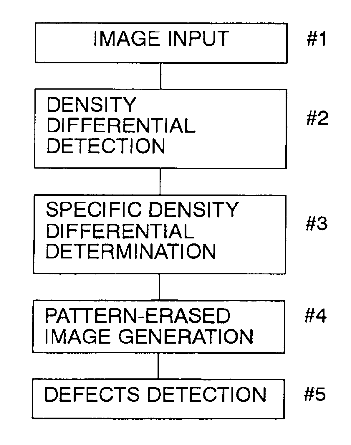
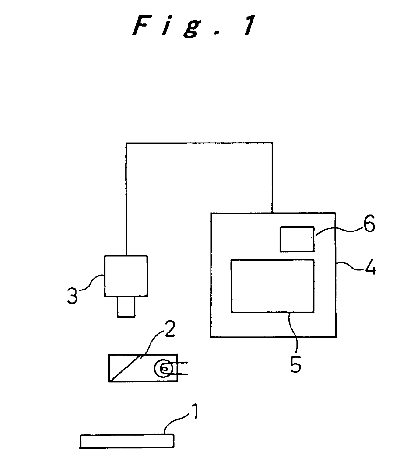
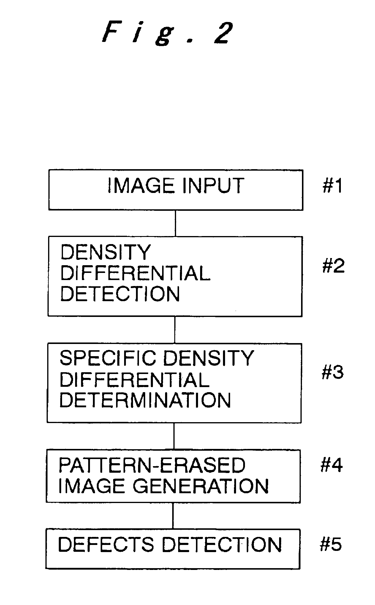
[0033]An embodiment in which a repeated pattern erasure method and pattern defect inspection device according to the present invention are applied to inspection of an electrode wiring glass panel in a liquid crystal array panel is described below with reference to FIG. 1 to FIG. 4.

[0034]In FIG. 1, which illustrates diagrammatically the construction of a pattern defect inspection device according to the present invention, the subject of inspection 1 is arranged in a prescribed position and is supplied with illumination by downward illumination 2, and an image thereof is picked up by an image pickup element comprising a CCD area sensor etc. The image data from the sensor pixels in image pickup element 3 is transferred, in one-to-one correspondence, to image memory 5 in a computer 4 constituting a processing device. The image data transferred into this image memory 5 is read to computer 4 and a processing program 6 is stored that performs prescribed processing. The image density is pro...


PUM

PropertyMeasurementUnit
distanceaaaaaaaaaa
densityaaaaaaaaaa
specific densityaaaaaaaaaa

Abstract

An image of a subject of inspection is picked up, and this image is demarcated into a plurality of areas. Density differences are found between reference pixels and a plurality of comparison pixels in the demarcated areas, and a density difference that is closest to 0 is determined as a specific density difference. The specific density difference is then applied to the reference density in the image of the subject, whereby repeated patterns in the image are erased.

Description

BACKGROUND OF THE INVENTION[0001]1. Technical Field of the Invention[0002]The present invention relates to a method of erasing repeated patterns and to a pattern defect detection device in image processing when detecting pattern defects contained in electronic equipment devices such as liquid crystal panels, plasma display panels, or semiconductor wafers.[0003]2. Description of Related Art[0004]Conventionally, inspection of pattern defects in the manufacture of electronic equipment devices such as liquid crystal panels, plasma or display panels or semiconductor wafers was performed by visual inspection by human beings or by automatic image processing carried out by machine.[0005]In the case of visual inspection, alterations in the type of electronic equipment being inspected can easily be coped with, and start-up is rapid, but there are the drawbacks that identifying the precise positions of defects takes time and throughput is poor. Maintaining and standardizing detection sensitivi...

Claims


Application Information

Patent Timeline
Patent Type & Authority Patents(United States)
IPC IPC(8): G01N21/956G01N21/88G06K9/00G06T7/00G06T1/00
CPCG06T7/0006G06T2207/30148
Inventor YUKAWA, NORIAKIKAWANO, HAJIMEAYAKI, YUKIHIRO
Owner PANASONIC CORP
Why Eureka
Try Eureka