
Method of manufacturing memory with nano dots

a manufacturing method and nano-dot technology, applied in the field of manufacturing memory with nano-dots, can solve problems such as difficulty in obtaining a uniform distribution of nano-dots

Active Publication Date: 2005-07-05
SAMSUNG ELECTRONICS CO LTD
View PDF3 Cites 29 Cited by
  • Summary
  • Abstract
  • Description
  • Claims
  • Application Information

AI Technical Summary

Problems solved by technology

However, this method is disadvantageous in that it is difficult to appropriately adjust sizes of the nano particles and, even if same-sized nano particles are selected and sprayed onto the substrate, it is difficult to obtain a uniform distribution of nano dots.

Method used


Image

  • Method of manufacturing memory with nano dots
  • Method of manufacturing memory with nano dots
  • Method of manufacturing memory with nano dots

Examples


Embodiment Construction

[0017]Korean Patent Application No. 2002-82387, filed on Dec. 23, 2002, and entitled, “Method Of Manufacturing Memory With Nano Dots,” is incorporated by reference herein in its entirety.

[0018]The present invention will be described more fully hereinafter with reference to the accompanying drawings, in which preferred embodiments of the invention are shown. The invention may, however, be embodied in different forms and should not be construed as being limited to the embodiments set forth herein. Rather, these embodiments are provided so that this disclosure will be thorough and complete, and will fully convey the scope of the invention to those skilled in the art. In the drawings, the thickness of layers and regions are exaggerated for clarity. It will also be understood that when a layer is referred to as being “on” another layer or substrate, it can be directly on the other layer or substrate, or intervening layers may also be present. Further, it will be understood that when a la...


PUM


Abstract

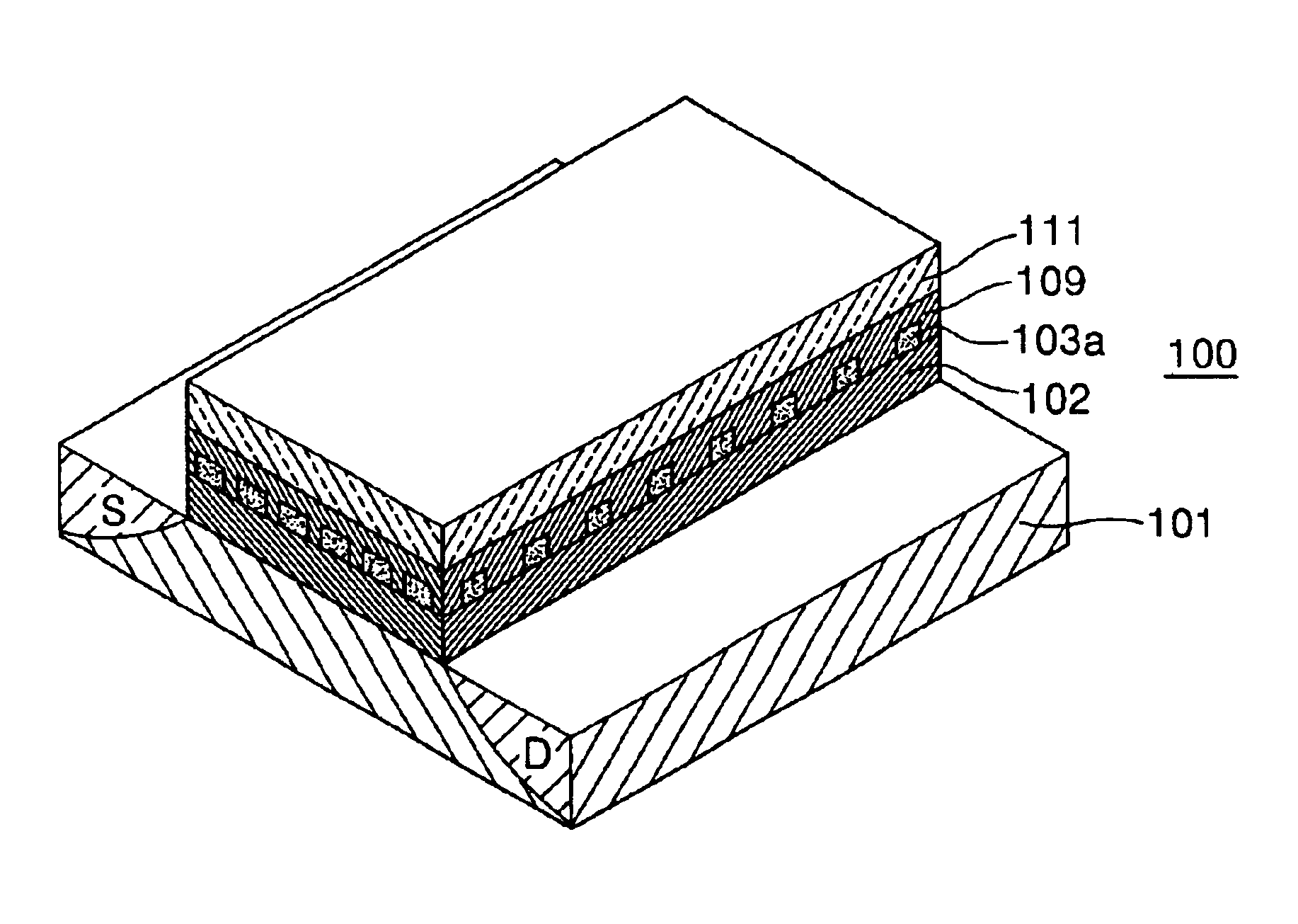
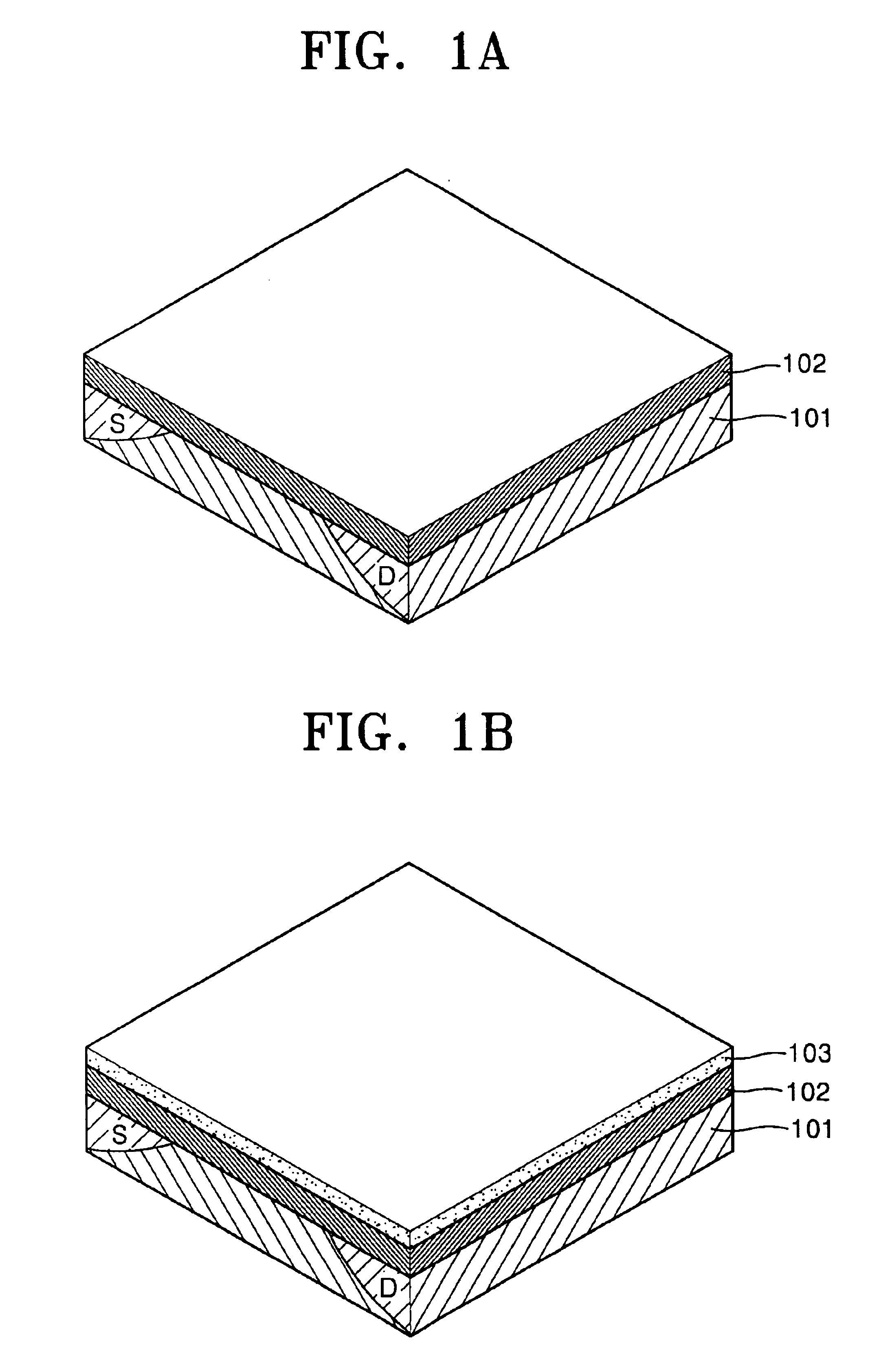
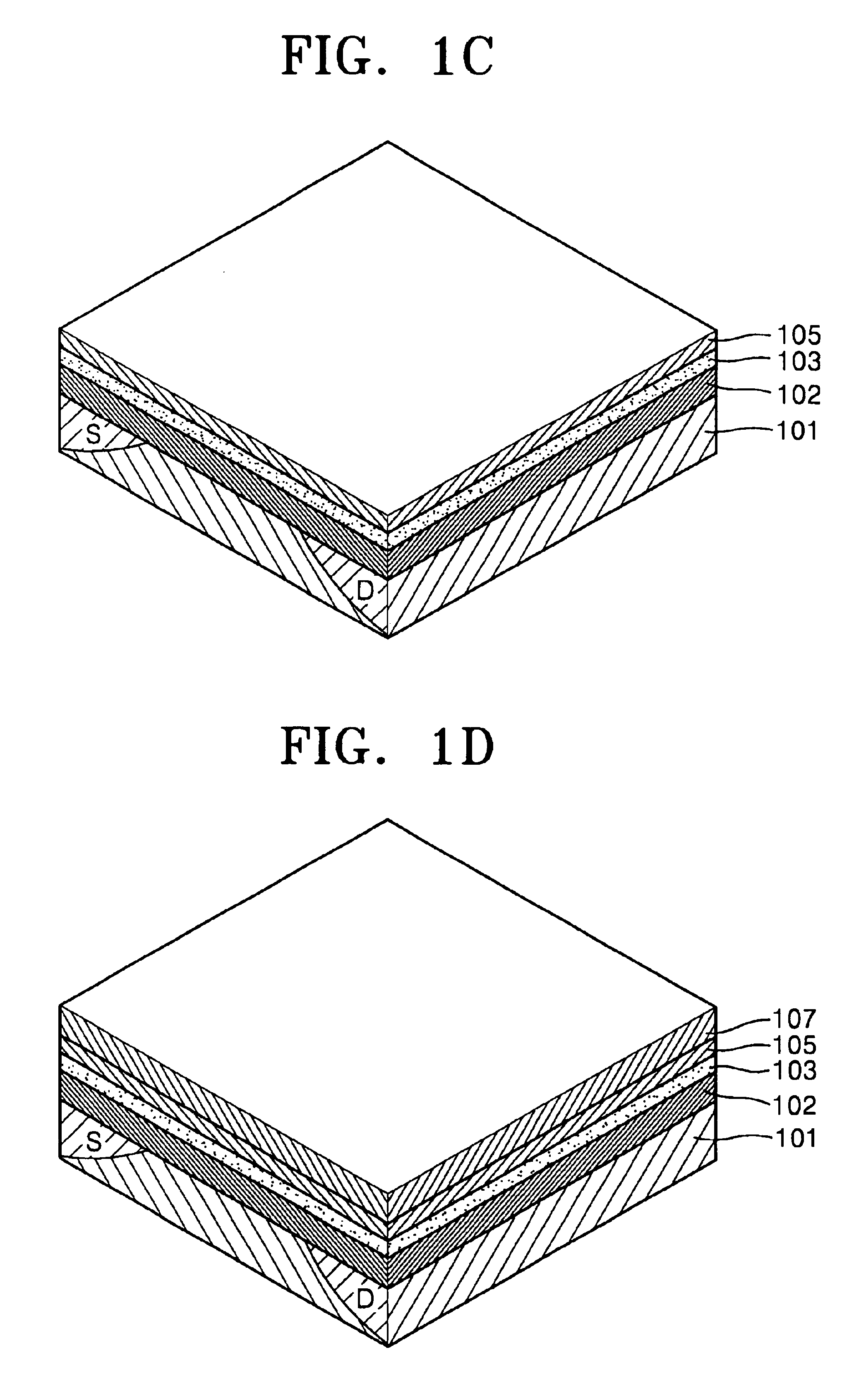
A method of fabricating memory with nano dots includes sequentially depositing a first insulating layer, a charge storage layer, a sacrificial layer, and a metal layer on a substrate in which source and drain electrodes are formed, forming a plurality of holes on the resultant structure by anodizing the metal layer and oxidizing portions of the sacrificial layer that are exposed through the holes, patterning the charge storage layer to have nano dots by removing the oxidized metal layer, and etching the sacrificial layer and the charge storage layer using the oxidized sacrificial layer as a mask, and removing the oxidized sacrificial layer, depositing a second insulating layer and a gate electrode on the patterned charge storage layer, and patterning the first insulating layer, the patterned charge storage layer, the second insulating layer, and the gate electrode to a predetermined shape, for forming memory having uniformly distributed nano-scale storage nodes.

Description

BACKGROUND OF THE INVENTION[0001]1. Field of the Invention[0002]The present invention relates to a method of manufacturing memory with nano dots. More particularly, the present invention relates to a method of manufacturing memory with nano dots using self-alignment.[0003]2. Description of the Related Art[0004]Currently, much attention and effort are being placed on the development of nano-scale devices to be included in apparatuses such as memory, laser diodes (LDs), photo diodes, transistors, far-ultraviolet detectors, solar batteries, and optical modulators. A number of electrons that are captured in a nanodevice depends on the size of nano dots. Nanodevices may be driven with a smaller amount of electrons than conventional devices, thereby lowering a threshold current. Therefore, a nanodevice can be driven by a low voltage and still produce a high output.[0005]Conventionally, nano dots are made by forming an atomic nucleus with Si or Si3N4 using a general deposition method such ...

Claims


Application Information

Patent Timeline
IPC IPC(8): H01L21/28H01L29/423H01L21/02H01L29/40H01L29/66H01L29/788H01L29/792B82B1/00H10B99/00H01L21/8247H01L29/06H10B69/00
CPCB82Y10/00H01L21/28273H01L21/28282H01L29/42332H01L29/7881H01L29/792Y10S977/723Y10S977/774H01L29/40114H01L29/40117H10B99/00
Inventor KIM, IN-SOOKSEO, SUN-AEYOO, IN-KYEONGJEONG, SOO-HWAN
Owner SAMSUNG ELECTRONICS CO LTD
Learn More