Transistor circuit

a transistor and circuit technology, applied in the field of transistor circuits, can solve the problems of defective pixels being typically deactivated, difficult to perfectly prevent such point defects, and pixel that cannot execute predetermined display operations, so as to increase the transistor capacitance, and increase the parasitic and/or channel capacitance of the second transistor.

Inactive Publication Date: 2005-07-05
SANYO ELECTRIC CO LTD
View PDF2 Cites 179 Cited by
  • Summary
  • Abstract
  • Description
  • Claims
  • Application Information

AI Technical Summary

Benefits of technology

[0014]An advantage of the present invention is that it provides an organic EL panel in which an operation test for each pixel can be conducted using an electrical charge measurement tester, so called array tester.
[0015]According to the present invention, parasitic and / or channel capacitance of a second transistor is increased. As a result, operation of the transistor can be confirmed by reading out charges stored in or discharged from the capacitance.
[0016]Further, operation of the transistor can be confirmed by configuring the parasitic and / or channel capacitance of the second transistor greater by a given degree compared to that of a storage capacitor, and reading out charges stored in or discharged from that capacitance.
[0017]It is preferable to increase the transistor capacitance by enlarging, in a planer direction, a portion of a channel region of the second transistor, such that the channel region is expanded while maintaining the channel width and channel length.

Problems solved by technology

In an organic EL panel as described above, a defect may occur during the manufacturing process of the panel in the two TFTs or other components constituting each pixel, resulting in a pixel that cannot execute predetermined display operations.
It is difficult to perfectly prevent such point defects which inevitably occur with a predetermined probability.
As a defect is visually unnoticeable when it merely generates a dark point in which no display is performed, a defective pixel is typically deactivated by disconnecting its wiring using a laser or the like.
However, this method is inefficient, requiring a long testing time.
However, as one pixel of an organic EL panel includes two TFTs, a test of the second TFT to determine whether an electric current is adequately supplied to the organic EL element (such that light emission results) cannot be inspected.

Method used


Image

  • Transistor circuit
  • Transistor circuit
  • Transistor circuit

Examples


Embodiment Construction

[0024]Preferred embodiments of the present invention will now be described with reference to the accompanying drawings.

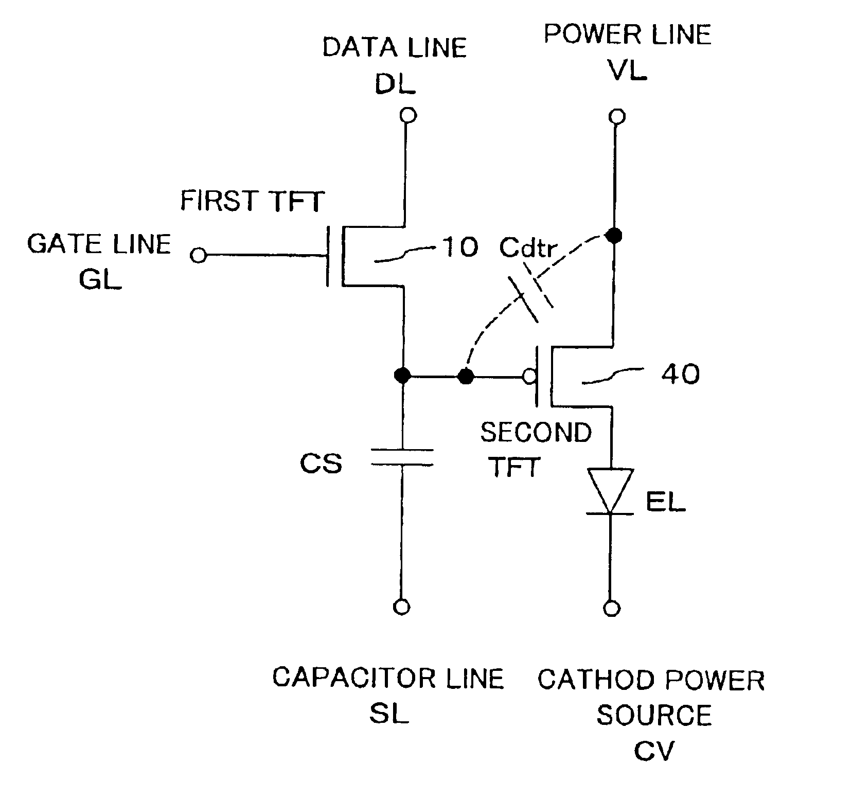
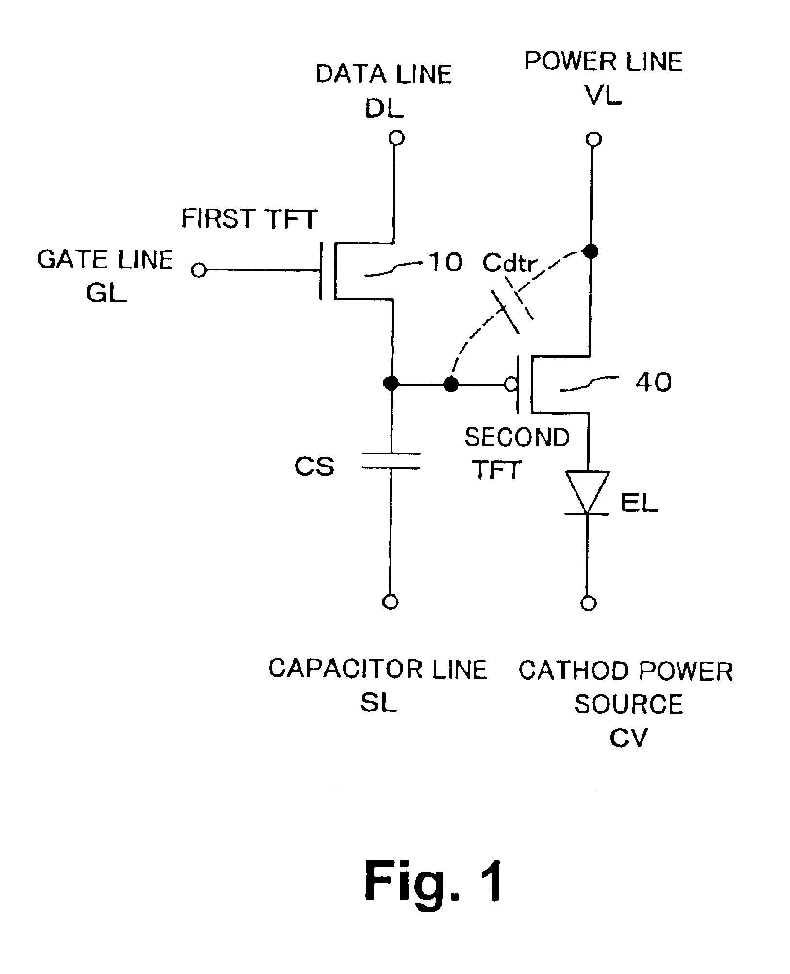
[0025]FIG. 1 shows a transistor circuit configuration for one pixel in an organic EL display panel. As in FIG. 5, the pixel of FIG. 1 comprises a first TFT 10, a storage capacitor CS, a second TFT 40, and an organic EL element EL. Further, the second TFT 40 inevitably includes a capacitance, namely, transistor capacitance Cdtr between the gate and the source and / or channel area of the second TFT 40.

[0026]According to the present embodiment, a test for determining whether the first TFT 10 and the second TFT 40 operate normally is conducted by turning on the first TFT 10 to allow charges to be stored in or discharged from the storage capacitor CS and the transistor capacitance Cdtr, and detecting an alteration in the capacitance value of the transistor capacitance Cdtr.

[0027]As is known, it is possible to determine whether the first TFT 10 operates normally by applyin...


PUM


Abstract

Transistor capacitance Cdtr inevitably generated between the gate and the drain of a second TFT is increased. Accordingly, an operation test of a first TFT and the second TFT can be conducted by turning on the first TFT to charge the transistor capacitance Cdtr and detecting the stored charges.

Description

BACKGROUND OF THE INVENTION[0001]1. Field of the Invention[0002]The present invention relates to a transistor circuit for driving various elements, and more particularly to a transistor circuit having its operation and inspection test facilitated.[0003]2. Description of the Related Art[0004]Transistors are commonly used for controlling supply and output of electric current in display devices and sensors.[0005]An example of a flat display panel is an organic EL display panel. An organic EL display panel is configured by arranging, in a matrix, a large number of pixels each composed of an organic EL element. One method for driving an organic EL element is the active matrix method in which a switching transistor is provided for each pixel, and display of each pixel is controlled by controlling the corresponding transistor.[0006]FIG. 5 shows an example circuit configuration of a pixel in an organic EL panel employing conventional thin film transistors (TFT). An organic EL panel is confi...

Claims


Application Information

Patent Timeline
Patent Type & Authority Patents(United States)
IPC IPC(8): H01L27/12H01L27/32H01L27/28H01L21/822G09G3/00G09G3/32H01L21/336H01L27/04H01L29/786
CPCG09G3/006G09G3/3225H01L27/12G09G2300/0842H01L27/3244H10K59/12G09G3/30
Inventor JINNO, YUSHI
Owner SANYO ELECTRIC CO LTD
Why Eureka
Try Eureka